May. 23, 2024

The Biden-Harris Administration announced that the U.S. Department of Commerce and Absolics, an affiliate of the Korea-based SKC, have signed a non-binding preliminary memorandum of terms to provide up to $75 million in direct funding under the CHIPS and Science Act to help advance U.S. technology leadership. The proposed investment would support the construction of a 120,000 square-foot facility in Covington, Georgia and the development of substrates technology for use in semiconductor advanced packaging. Started through a collaboration with the 3D Packaging Research Center at Georgia Tech, Absolics’ project serves as an example of American lab-to-fab development and production.
"Glass-core packaging holds the promise to revolutionize the field of advanced packaging and impact major paradigms such as artificial intelligence, mm-wave/THz communication, and photonic connectivity," said Muhannad Bakir, Dan Fielder Professor in the School of Electrical and Computer Engineering and Director of the 3D Systems Packaging Research Center at Georgia Tech. "We look forward to supporting Absolics in establishing a glass-core packaging facility in the State of Georgia through workforce development initiatives."
Because of President Biden’s CHIPS and Science Act, this proposed investment would support over an estimated 1,000 construction jobs and approximately 200 manufacturing and R&D jobs in Covington and enhance innovation capacity at Georgia Institute of Technology, supporting the local semiconductor talent pipeline.
The proposed investment with Absolics is the first proposed CHIPS investment in a commercial facility supporting the semiconductor supply chain by manufacturing a new advanced material.
News Contact
Amelia Neumeister
Research Communications Program Manager
Apr. 22, 2024

Effective July 1, Eric Vogel will become the executive director of the Institute for Matter and Systems (IMS), Georgia Tech’s newest Interdisciplinary Research Institute (IRI) that will launch on the same date.
As an evolution of the Institute for Materials (IMat) and the Institute for Electronics and Nanotechnology (IEN), IMS aims to enable convergent research at Georgia Tech related to the science, technology, and societal underpinnings of innovative materials and devices. Additionally, IMS seeks to integrate these innovations into systems that enhance human well-being and performance across information and communication, the built environment, and human-centric technologies that improve human health, wellness, and performance.
“Executive Vice President for Research Chaouki Abdallah and I are very excited about the launch of IMS, which positions Georgia Tech for integration of science and technology from atoms to devices, while explicitly drawing in researchers in the social sciences, design, business, and computing,” said Vice President of Interdisciplinary Research Julia Kubanek.
“IMS will ensure relevance across Georgia Tech through its newly configured Internal Advisor and Ambassador Board with representation across all six Colleges and GTRI,” she said. “Additional advisory committees representing IMS employees and facility users will ensure that we don’t sacrifice any of the research excellence for which IEN and IMat are known. With IMS I expect we will be even better positioned to tackle research problems that will have the greatest positive societal impact.”
Vogel will continue in his current position as the executive director of IMat until the launch of IMS. In addition to leading and growing IMat, Vogel is the Hightower Professor of Materials Science and Engineering at Georgia Tech’s School of Materials Science and Engineering, and he served as the IEN deputy director prior to leading IMat.
“It is an honor to be appointed executive director of the Institute for Matter and Systems, and I look forward to collaborating with the talented faculty and staff associated with it,” said Vogel. “This opportunity allows us to leverage the core competencies of IEN and IMat while extending our capabilities beyond nanotechnology and materials science. Together, we will be a hub for interdisciplinary research ranging from advanced materials to complex systems that solve global challenges.”
Georgia Tech’s IRIs facilitate collaboration between researchers and students from its six Colleges, the Georgia Tech Research Institute, national laboratories, and corporate entities to tackle critical topics of strategic significance for the Institute as well as for local, state, national, and international communities. IMS will also house and maintain the state-of-the-art Materials Characterization Facility and one of the largest academic cleanrooms in the nation, which offers a broad range of fabrication capabilities from basic discovery to prototype realization.
Before joining Georgia Tech in 2011, Vogel was an associate professor of materials science and engineering and electrical engineering at the University of Texas at Dallas. During this time, he also served as the associate director of the Texas Analog Center of Excellence and led UT Dallas’s involvement in the Southwest Academy for Nanoelectronics.
Prior to UT Dallas, he led the CMOS and Novel Devices Group and established the Nanofabrication Facility at the National Institute of Standards and Technology. Vogel holds a Ph.D. in electrical engineering from North Carolina State University and a B.S. in electrical engineering from the Pennsylvania State University. His research focuses on the development and fundamental understanding of electronic and nanomaterials and devices.
News Contact
Laurie Haigh
Research Communications
Apr. 19, 2024
 sandwiched by 2D materials (including h-BN).</p>")
Electrostatic capacitors realized with ferroelectric single crystalline BaTiO3 (BTO) sandwiched by 2D materials (including h-BN).
Metz, France
Three-dimensional (3D) hetero-integration technology is set to transform the field of electronics. Vertically stacking functional layers, creates novel 2D-3D circuit architectures with high integration density and unprecedented multifunctionality.
Three researchers at Georgia Tech-CNRS IRL 2958, a joint international research laboratory based at Georgia Tech-Europe in Metz, France, were among a team that demonstrated cutting-edge 2D/single-crystalline 3D/2D (2D/C-3D/2D) Integration using a precise layer splitting technique to overcome drawbacks in ferroelectric materials use in electrostatic capacitors.
Abdallah Ougazzaden, professor of Electrical and Computer Engineering at Georgia Tech, and president of Georgia Tech-Europe, Phuong Vuong, Georgia Tech-CNRS IRL 2958 researcher, and Suresh Sundaram, adjunct faculty in Georgia Tech’s School of Electrical and Computer Engineering, are co-authors on an April 19, 2024 research article in the journal, Science, entitled “High energy density in artificial heterostructures through relaxation time modulation.”
Ferroelectric materials used in electrostatic capacitors have unique advantages such as maximum polarization due to their higher electric susceptibilities related to dielectric constants, or permittivity, a measure of a material’s ability to store electrical energy. However, their high remnant polarization, the amount of polarization that remains in the material after the electric field is removed, limits how well they can store and release energy during the discharging process.
In the Science article, researchers demonstrated an innovative approach that sandwiches a single crystalline BTO (C-BTO) layer with 2D materials in the form of a freestanding membrane and effectively suppresses the remnant polarization of ferroelectric materials while maintaining the maximum polarization.
This ultra-thin vertical stacking technology was achieved using three different two-dimensional materials in combination with single crystalline BTO (C-BTO). Hexagonal boron nitride semiconductor was developed in the International Research Laboratory at GT-Europe, while graphene, and Molybdenum disulfide (MoS2) were developed at MIT.
These new 2D material technologies have a special type of bonding called van der Waals forces. On account of this, the layers can be easily separated to create components without needing any chemical etching or cutting processes.
“The 2D hexagonal boron nitride (h-BN) material that we are developing at Georgia Tech-CNRS IRL 2958 on large surfaces using the MOCVD epitaxial growth technique has demonstrated its significant potential in emerging technologies across various domains such as future quantum computers, biotechnology, flexible electronics, sensors, energy, and optogenetics.” said Ougazzaden, head of the h-BN project at Georgia Tech-CNRS IRL 2958,” adding, “We are currently working on some of these applications, and we hope to produce even more results and demonstrate new achievements."
Electrostatic capacitors, with their ability to store and release electrical energy quickly, find a wide range of applications across various fields of electronics and electrical engineering for energy storage, power conditioning etc.
In a similar collaboration, the same research team from Georgia Tech-CNRS IRL 2958 published a paper in December 2023, showing the first demonstration of the monolithic 3D integration of an artificial intelligence (AI) processor using two-dimensional (2D) materials.
This innovative integration approach combined six layers of transistor and memristor networks into a 3D nano-system. By stacking nanoscale materials made from 2D materials using bottom-up technology, the team created a fully integrated AI system.
The monolithic 3D method significantly improved processing efficiency by reducing time, voltage drops, latency, and footprint. In addition to offering a solution for electronic hetero-integration with 2D materials, broke new ground for advanced multifunctional processors and systems for AI applications and complex computing.
The team’s results on vertical hetero-integration were published in the scientific journal, Nature Materials, entitled, "Monolithic 3D Integration of 2D Materials-Based Electronics towards Ultimate Edge Computing Solutions.”
The researchers who contributed to the Science article discovered that when ferroelectric materials are combined in special structures (like 2D/C-3D/2D layers), it affects how much leftover charge a capacitor has and how well it can store energy. These insights will advance designs of high-energy capacitors using these materials. In the future, this could lead to more efficient and powerful energy storage systems.
Mar. 12, 2024

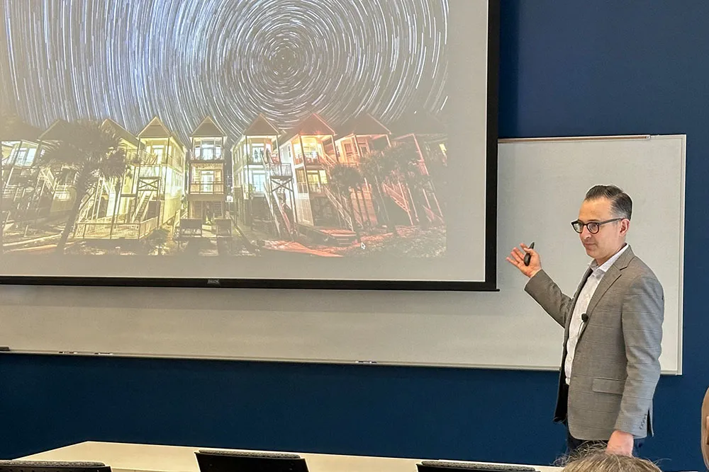
Muhannad Bakir has been named director of the Institute for Electronics and Nanotechnology’s 3D Systems Packaging Research Center (PRC).
"We’re thrilled to have Professor Bakir joining us as the new director,” said Michael Filler, IEN’s interim executive director. “His wealth of experience and pioneering work in advanced packaging make him an excellent fit to lead the PRC into an exciting new era of innovation and technological impact.”
Originating as a National Science Foundation Engineering Research Center in 1993, the PRC is a national leader in the advanced packaging of microelectronics. Advanced packaging in microelectronics refers to innovative techniques for merging and interconnecting multiple components within a single electronic entity. This enables more powerful, efficient, and versatile microelectronic systems, driving innovation across various industries. The Center conducts research and education in all aspects of electronics packaging, including design, materials, process, assembly, thermal management, and system integration. Its work is driven by a wide range of applications, such as high-performance computing, artificial intelligence, automotive systems, wireless communications, and space exploration.
“I am honored for the opportunity to lead the PRC and look forward to working with the campus community and our industry, government, and academic partners on a research agenda that tackles the multifaceted challenges in advanced packaging and heterogeneous integration,” said Bakir.
As director, Bakir will guide the PRC into the future of advanced packaging through his vision and expertise. He is responsible for ensuring that the PRC's world-class facilities support the emerging needs of advanced packaging of microelectronics and supports members of the campus community who uses these facilities.
“We are excited to lead the science and engineering that culminates in system level prototyping and demonstrators for AI, mm-wave, photonic systems, and beyond,” he said.
Bakir, who also serves as the Dan Fielder Professor in the School of Electrical and Computer Engineering and leads the Integrated 3D Systems Group, brings a wealth of experience to his new role as PRC director. He and his research group have received more than 30 paper and presentation awards including seven from the IEEE Electronic Components and Technology Conference, four from the IEEE International Interconnect Technology Conference, and one from the IEEE Custom Integrated Circuits Conference. His group was also awarded the 2014 and 2017 Best Papers of the IEEE Transactions on Components Packaging and Manufacturing Technology.
Bakir is the recipient of the 2013 Intel Early Career Faculty Honor Award, 2012 DARPA Young Faculty Award, 2011 IEEE CPMT Society Outstanding Young Engineer Award, and was an Invited Participant in the 2012 National Academy of Engineering Frontiers of Engineering Symposium. He is the co-recipient of the 2018 IEEE Electronics Packaging Society Exceptional Technical Achievement Award “for contributions to 2.5D and 3D IC heterogeneous integration, with a focus on interconnect technologies.” He is also the co-recipient of the 2018 McKnight Foundation Technological Innovations in Neuroscience Awards. In 2020, Bakir received the Georgia Tech Outstanding Doctoral Thesis Advisor Award.
He serves as a senior area editor for the IEEE Transactions on Components, Packaging and Manufacturing Technology and was previously an Editor for IEEE Transactions on Electron Devices. He has also served as a distinguished lecturer for IEEE EPS.
News Contact
Amelia Neumeister
Research Communications Program Manager
Mar. 04, 2024

The Institute for Electronics and Nanotechnology (IEN) at Georgia Tech has announced the 2023 IEN Exponential Electronics (IEN-EX) Seed Grant winner, Vida Jamali, Assistant Professor in the School of Chemical and Biomolecular Engineering at Georgia tech.
The primary purpose of this program is to give early-stage research and development to create revolutionary electronic systems.
IEN-EX provides seed funding for Georgia Tech researchers to pursue “1000x” ideas within electronics or that bridge electronics with other technical domains. “1000x” ideas are those with the potential to improve one or more well-defined, but often overlooked or underappreciated performance metrics by at least 1000x.
In this brief Q&A, Jamali discusses her research focus, how it relates to electronics research, and the impact of this initiative.
- What is your field of expertise and at what point in your life did you first become interested in this area? In situ liquid phase transmission electron microscopy. I started learning about this tool when I was a postdoc to develop it as a single particle tracking method.
- Briefly explain your research: My research is focused on investigating the dynamics of nanoscale objects in their native liquid environment, from synthetic colloidal nanomachines to biological macromolecules, using liquid phase transmission electron microscopy. We develop experimental and computational tools to visualize and characterize dynamic behavior (equilibrium and non-equilibrium) at small length scales and in real-time.
- Who are the PIs: Me and Amirali Aghazadeh, Assistant Professor in the School of Electrical and Computer Engineering.
- What questions or challenges sparked your current research? Is it possible to use an electron microscope and capture the dynamics of nanoscale materials in time as they move and interact with each other and respond to their surrounding environment with a high spatiotemporal resolution?
- How is your research working to create revolutionary electronic systems? We design and develop a new nanoelectronic coded aperture device that once integrated into transmission electron microscopes can increase resolution exponentially.
- What are the broader global and social benefits of the research you and your team conduct? Once realized this technology opens a new window into dynamic phenomena at a scale inaccessible before. This unprecedented level of information will significantly advance areas from drug discovery impacting human health to achieving single crystalline materials for the semiconductor industry.
- How will this funding support your research? This funding will support graduate students who will be realizing this idea
News Contact
Amelia Neumeister
Research Communications Program Manager
Feb. 28, 2024
The Oliver Brand Memorial Technical Symposium was held on Feb. 22 at the Georgia Institute of Technology in honor of the technical achievements of Professor Oliver Brand.
The event brought together students, faculty, and professionals in the microelectromechanical systems research community to celebrate Brand’s contributions to the field and explore cutting-edge research.
“As a fellow academic, looking at his contributions, they’re remarkable,” said Mike Filler, interim executive director of the Institute for Electronics and Nanotechnology (IEN). “But then what put it over the top was his humanity. He supported every member of the community; he believed in people and had their best interests in mind.”
The seven speakers included research colleagues, graduate students and technical staff who worked closely with Brand throughout his career. They reminisced about Brand and discussed the research and technical achievements they collaborated on with him.
Brand spent more than 20 years as a member of the Georgia Tech faculty. In addition to leading IEN, he was a professor in the School of Electrical and Computer Engineering, director of the Coordinating Office for the NSF-funded National Nanotechnology Coordinated Infrastructure (NNCI), and director of the Southeastern Nanotechnology Infrastructure Corridor, one of the 16 NNCI sites.
Brand united researchers in the fields of electronics and nanotechnology, fostering collaboration and expanding IEN to include more than 200 faculty members. In addition to his respected work in the field of microelectromechanical systems, he is remembered for his kindness, dedication, and unwavering support toward all who knew him.
News Contact
Amelia Neumeister
Research Communications Program Manager
Feb. 21, 2024

Energy is everywhere, affecting everything, all the time. And it can be manipulated and converted into the kind of energy that we depend on as a civilization. But transforming this ambient energy (the result of gyrating atoms and molecules) into something we can plug into and use when we need it requires specific materials.
These energy materials — some natural, some manufactured, some a combination — facilitate the conversion or transmission of energy. They also play an essential role in how we store energy, how we reduce power consumption, and how we develop cleaner, efficient energy solutions.
“Advanced materials and clean energy technologies are tightly connected, and at Georgia Tech we’ve been making major investments in people and facilities in batteries, solar energy, and hydrogen, for several decades,” said Tim Lieuwen, the David S. Lewis Jr. Chair and professor of aerospace engineering, and executive director of Georgia Tech’s Strategic Energy Institute (SEI).
That research synergy is the underpinning of Georgia Tech Energy Materials Day (March 27), a gathering of people from academia, government, and industry, co-hosted by SEI, the Institute for Materials (IMat), and the Georgia Tech Advanced Battery Center. This event aims to build on the momentum created by Georgia Tech Battery Day, held in March 2023, which drew more than 230 energy researchers and industry representatives.
“We thought it would be a good idea to expand on the Battery Day idea and showcase a wide range of research and expertise in other areas, such as solar energy and clean fuels, in addition to what we’re doing in batteries and energy storage,” said Matt McDowell, associate professor in the George W. Woodruff School of Mechanical Engineering and the School of Materials Science and Engineering (MSE), and co-director, with Gleb Yushin, of the Advanced Battery Center.
Energy Materials Day will bring together experts from academia, government, and industry to discuss and accelerate research in three key areas: battery materials and technologies, photovoltaics and the grid, and materials for carbon-neutral fuel production, “all of which are crucial for driving the clean energy transition,” noted Eric Vogel, executive director of IMat and the Hightower Professor of Materials Science and Engineering.
“Georgia Tech is leading the charge in research in these three areas,” he said. “And we’re excited to unite so many experts to spark the important discussions that will help us advance our nation’s path to net-zero emissions.”
Building an Energy Hub
Energy Materials Day is part of an ongoing, long-range effort to position Georgia Tech, and Georgia, as a go-to location for modern energy companies. So far, the message seems to be landing. Georgia has had more than $28 billion invested or announced in electric vehicle-related projects since 2020. And Georgia Tech was recently ranked by U.S. News & World Report as the top public university for energy research.
Georgia has become a major player in solar energy, also, with the announcement last year of a $2.5 billion plant being developed by Korean solar company Hanwha Qcells, taking advantage of President Biden’s climate policies. Qcells’ global chief technology officer, Danielle Merfeld, a member of SEI’s External Advisory Board, will be the keynote speaker for Energy Materials Day.
“Growing these industry relationships, building trust through collaborations with industry — these have been strong motivations in our efforts to create a hub here in Atlanta,” said Yushin, professor in MSE and co-founder of Sila Nanotechnologies, a battery materials startup valued at more than $3 billion.
McDowell and Yushin are leading the battery initiative for Energy Materials Day and they’ll be among 12 experts making presentations on battery materials and technologies, including six from Georgia Tech and four from industry. In addition to the formal sessions and presentations, there will also be an opportunity for networking.
“I think Georgia Tech has a responsibility to help grow a manufacturing ecosystem,” McDowell said. “We have the research and educational experience and expertise that companies need, and we’re working to coordinate our efforts with industry.”
Marta Hatzell, associate professor of mechanical engineering and chemical and biomolecular engineering, is leading the carbon-neutral fuel production portion of the event, while Juan-Pablo Correa-Baena, assistant professor in MSE, is leading the photovoltaics initiative.
They’ll be joined by a host of experts from Georgia Tech and institutes across the country, “some of the top thought leaders in their fields,” said Correa-Baena, whose lab has spent years optimizing a semiconductor material for solar energy conversion.
“Over the past decade, we have been working to achieve high efficiencies in solar panels based on a new, low-cost material called halide perovskites,” he said. His lab recently discovered how to prevent the chemical interactions that can degrade it. “It’s kind of a miracle material, and we want to increase its lifespan, make it more robust and commercially relevant.”
While Correa-Baena is working to revolutionize solar energy, Hatzell’s lab is designing materials to clean up the manufacturing of clean fuels.
“We’re interested in decarbonizing the industrial sector, through the production of carbon-neutral fuels,” said Hatzell, whose lab is designing new materials to make clean ammonia and hydrogen, both of which have the potential to play a major role in a carbon-free fuel system, without using fossil fuels as the feedstock. “We’re also working on a collaborative project focusing on assessing the economics of clean ammonia on a larger, global scale.”
The hope for Energy Materials Day is that other collaborations will be fostered as industry’s needs and the research enterprise collide in one place — Georgia Tech’s Exhibition Hall — over one day. The event is part of what Yushin called “the snowball effect.”
“You attract a new company to the region, and then another,” he said. “If we want to boost domestic production and supply chains, we must roll like a snowball gathering momentum. Education is a significant part of that effect. To build this new technology and new facilities for a new industry, you need trained, talented engineers. And we’ve got plenty of those. Georgia Tech can become the single point of contact, helping companies solve the technical challenges in a new age of clean energy.”
News Contact
Feb. 15, 2024

The Georgia Institute of Technology today announced the signing of a master research agreement with Micron Technology, a global leader in memory and storage solutions. Under the new agreement, the two organizations will expand their collaborative efforts in providing students with experiential research opportunities and expanding access to engineering education.
“We are proud to join forces with Georgia Tech, home to some of the nation’s top programs, to expand students’ opportunities in STEM education,” said Scott DeBoer, executive vice president of Technology and Products at Micron. “This collaboration will help push the boundaries in memory technology innovation and ensure we prepare the workforce of the future.”
“We believe that when academia and industry converge, the best ideas flourish into game-changing innovations,” said Chaouki T. Abdallah, executive vice president for Research at Georgia Tech. “The synergy between Micron and Georgia Tech has already been tremendously fruitful, and we are so excited for the boundless opportunities on our shared horizon.”
“The signing of the master research agreement represents a significant step towards increasing additional collaboration pathways between Micron and GT including the joint pursuit of major federal funding activities, technology transfer, student internships and technology transfer,” said George White, senior director of Strategic Partnerships at Georgia Tech.
The first project under the agreement is already underway. Saibal Mukhopadhyay, professor in the School of Electrical and Computer Engineering, is leading the research efforts titled “Configurable Processing-In-Memory.” This cutting-edge research will enable memory devices to work faster and more efficiently.
News Contact
Amelia Neumeister
Research Communications Program Manager
Jan. 11, 2024

In 1950, Alan Turing asked, “Can machines think?” More than 70 years later, advancements in artificial intelligence are creating exciting possibilities and questions about its potential pitfalls.
A recent executive order issued by President Joe Biden seeks to establish "new standards for AI safety and security" while addressing consumer privacy concerns and promoting innovation. Georgia Tech experts have examined the key elements of the order and offer their thoughts on its scope and what comes next.
A Precautionary Tale
The order calls for the development of standards, tools, and tests to ensure the safe use of AI. From voice scams and phishing campaigns to larger-scale threats, the technology’s potential dangers have been widely documented. But Margaret Kosal, associate professor in the Ivan Allen College of Liberal Arts, says that additional context is often needed to dispel hysteria.
"No one is going to be hooking up AI to launch nuclear weapons, but AI capabilities may enable targeting, or enable the command and control and the decision-making time to be compressed,” she said.
The order will create an AI Safety and Security Board tasked with addressing critical threats. Companies developing foundation models that "pose a serious risk to national security, national economic security, or national public health and safety” will be required to notify the federal government when training the model and required to share the results of all red-team safety tests — a simulated cyberattack to test a system's defenses.
Since the launch of ChatGPT in 2022, a CNBC report details a 1,267% rise in phishing emails. Srijan Kumar, assistant professor in the College of Computing, attributes the increase to the technology's availability and an inability to rein in "bad actors."
He says these scams will only continue to get more sophisticated and personalized. They “can be created by knowing what you might be willing to fall prey to versus what I might fall prey to,” said Kumar, whose systems have influenced misinformation detection on sites like X (formerly Twitter) and Wikipedia. “AI is not going to autonomously do all of those bad things, but this order can ensure there are consequences for people who misuse it.”
A Delicate Balance
Building an AI platform requires large amounts of data regardless of its intended application. Two primary goals of the executive order are protecting privacy and advancing equity.
To protect personal data, the order tasks Congress with evaluating how agencies collect and use commercially available information and address algorithmic discrimination.
Acknowledging that everyone should be allowed to have their voice represented in the outputs of AI data sets, Deven Desai, associate professor in the Scheller College of Business, noted, "There are people who don't want to be part of data sets, which is their right, but this means their voices won't be reflected in the outputs.”
The order also includes sections to address intellectual property concerns among inventors and creators, though legal challenges will likely set new precedents in the years ahead.
When that time comes, Kosal says that defining “theft” in the context of AI becomes the true challenge and that, ultimately, money will play a significant role. "If you spit out a Harry Potter book and read it yourself, nobody will care. It's when you start selling it to make money, and you don't share proceeds with the original people, then it becomes an issue," she said.
What Does AI-Generated Mean?
The order instructs the Department of Commerce to develop guidelines for content authentication and watermarking to label AI-generated content. Desai questions what it means for something to be truly created by AI.
An important distinction lies between using AI to assist a writer in organizing their thoughts and using the technology to generate content. He likens the trend to the music industry in the 1980s.
"Synthesizers really changed people's ability to generate music and, for a while, people thought that was horrible. They can just program the music. They're not. I am still the human responsible for that music, or that article in this case, so what is the point of the label?" he asks.
As AI assistance becomes commonplace in content creation, trusting the source of information is increasingly important. Recently, articles published on Sports Illustrated's website featured AI-generated content provided by a third-party company that had used a machine to write the content and create fake bylines. Sports Illustrated, which may not have known of the problem, ran the material without disclosure to readers. CEO Ross Levinsohn was ousted shortly after the story broke.
“Perhaps if the third party had disclosed its use of AI software, SI would have been able to assess how much AI was used and then chosen not to run the material, or to run it with a disclaimer that AI helped write the material,” Desai said. "Of course, even if they label the content as AI-generated, a reader still won't know exactly how much of the content came from AI or a human.”
AI and the Workforce
As AI systems and models become more sophisticated, workers may become more concerned about being replaced. To counteract these concerns, the order calls for a study to examine AI’s potential impact on labor markets and investments in workforce training efforts.
Kumar compares the rise of AI to similar technological innovations throughout history and sees it as an opportunity for workers and industries to adapt. "It's less a matter of AI replacing workers and more of reskilling people to use the new technology. It's no different from when assembly lines in the auto industry were created."
Promoting Innovation and Competition
The power to harness the full potential of AI has initiated a race to the top. Desai believes that part of the executive order providing resources to smaller developers can help level the playing field.
"There is a possibility here for markets to open up. Current players using models that weren't built with transparency in mind might struggle, but maybe that's OK."
The issue of reliability and transparency comes into focus for Desai, especially as it relates to government usage of AI. The order calls on agencies to "acquire specified AI products and services faster, more cheaply, and more effectively through more rapid and efficient contracting."
When taxpayer dollars are at stake, government can’t afford to trust a technology it doesn’t fully understand — a topic Desai has explored elsewhere. "You can’t just say, ‘We don’t know how it works, but we trust it.’ That’s not going to work. So that’s where there may be a slowdown in the government’s ability to use private sector software if they can’t explain how the thing works and to show that it doesn’t have discriminatory issues.”
What's Next
Promoting and policing the safe use of AI cannot be done independently. Georgia Tech experts agree that participation on a global scale is necessary. To that end, the European Union will unveil its comprehensive EU AI Act, which includes a similar framework to the president's executive order.
Due to the evolving nature of AI, the executive order or the EU's actions will not be all-encompassing. Law often lags behind technology, but Kosal points out that it's crucial to think beyond what currently exists when crafting policy.
Experts also agree that AI cannot be regulated or governed through a single document and that this order is likely the first in a series of policymaking moves. Kosal sees tremendous opportunity with the innovation surrounding AI but hopes the growing fear of its rise does not usher in another AI winter, in which interest and research funding fade.
News Contact
Steven Gagliano - Institute Communications
Dec. 05, 2023
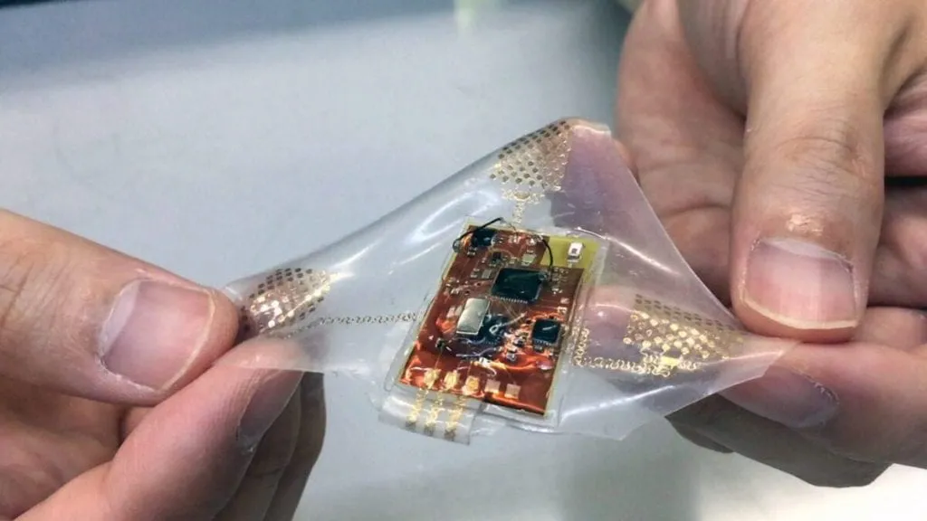

A new research center in the Institute for Electronics and Nanotechnology (IEN) will help bring together human-centered bioelectronics technology research to improve human healthcare and expand human-machine interface technologies.
The Wearable Intelligent Systems and Healthcare (WISH) Center will work to push innovation in wearable sensors and electronics technologies. Focus areas of the center will include electronics, artificial intelligence, biological science, material sciences, manufacturing, system design, and medical engineering.
“We are excited by the promise of bioelectronics improving human health and all the exciting science engineering that is required to make it a reality,” said Michael Filler, interim executive director of IEN.
WISH is directed by W. Hong Yeo, associate professor in Georgia Tech’s George W. Woodruff School of Mechanical Engineering and the Wallace H. Coulter Department of Biomedical Engineering at Georgia Tech and Emory, and Yuhang Hu, associate professor in the School of Chemical and Biomolecular Engineering at Georgia Tech.
“I founded WISH to bring together Georgia Tech’s expertise in various disciplines and to create opportunities for developing wearable bioelectronics and human-machine technologies leading to better lives and communities,” said Yeo.
Yeo’s research focuses on developing soft sensors, electronics and robotics for health monitoring and disease diagnosis at the intersection of human and machine interaction. Other researchers in the center represent disciplines from across Georgia Tech’s Colleges of Engineering, Computing, Sciences, Design, and Liberal Arts; Emory University; and Children’s Healthcare of Atlanta.
WISH will be one of IEN’s 10 strategic research centers, along with the 3D Systems Packaging Research Center, a graduated NSF Engineering Research Center focusing on advanced packaging using 2.5D and 3D heterogeneous integration technologies, and the Georgia Electronic Design Center, one of the world’s largest university-based semiconductor research centers. WISH is an evolution of the Center for Human-Centric Interfaces and Engineering, which received seed funding from IEN to focus on collaborative research for human-centered design, biofeedback control, and integrated nanosystems to advance human-machine interaction in the scope of healthcare.
IEN supports early-stage research in underfunded research areas that span all disciplines in science and engineering through its seed grant programs, which focus on research in biomedicine, electronics, optoelectronics and photonics, and energy applications.
News Contact
Amelia Neumeister, Research Communications