Jul. 09, 2025
 wafer used in a multi-chip module featuring 3D optical interconnects. <em>(Photo: Allison Carter)</em></p>")
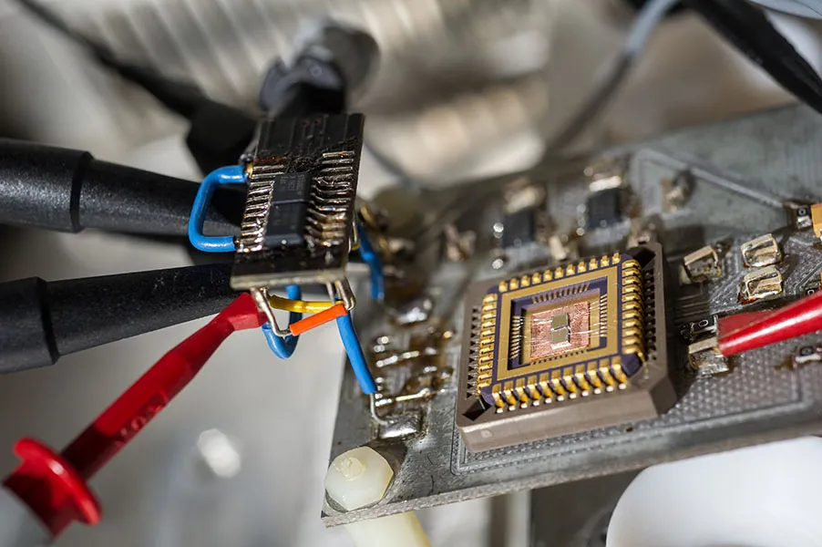
Silicon-on-insulator (SOI) wafer used in a multi-chip module featuring 3D optical interconnects. (Photo: Allison Carter)
 multi-layer planar waveguides, 2) free-form couplers, and 3) a dense vertical waveguide array.</p>")
A schematic illustration of a multi-chip structure with 3D optical routing. The key parts of Adibi's proposed system are: 1) multi-layer planar waveguides, 2) free-form couplers, and 3) a dense vertical waveguide array.
</em></p></div></div></div>")
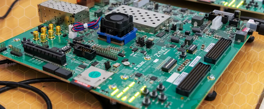
By combining advanced optical techniques, Professor Ali Adibi’s 3D optical routing systems looks to enable vertical chip integration in a way not previously achieved. (Photo: Allison Carter)
The future of computing is lit, literally.
As microchips grow more complex and data demands intensify, traditional electrical connections are hitting their limits. Speed is king in today’s digital systems, but a major bottleneck remains in how quickly information can move between components like processors and memory.
This lag is one of the most pressing challenges in advanced hardware design. While processors continue to accelerate, the links that connect them can't keep pace.
Georgia Tech researcher Ali Adibi is addressing this problem with $5.3 million in funding over three years from the Defense Advanced Research Projects Agency (DARPA). His project is part of DARPA’s Heterogeneous Adaptively Produced Photonic Interfaces (HAPPI) program, which aims to dramatically boost the speed and density of data transmission within microsystems by using light instead of electricity.
“Optical solutions are highly advantageous for providing the required data rates and power consumptions, and our project is formed to address the most important challenges for achieving the system-level performance,” said Adibi, a professor and Joseph M. Pettit Chair in the School of Electrical and Computer Engineering.
The project brings together a multidisciplinary team, including collaborators from the Massachusetts Institute of Technology, University of Florida, NY CREATES, and NHanced Semiconductors, Inc.
Going Vertical
Unlike traditional optical communication, which connects systems across distances, this project focuses on enabling ultra-fast, low-loss communication withinelectronic systems.
The key innovation is vertically connecting electronic chips in a compact stack. This design helps overcome the limitations of planar optical routing geometries (layouts that guide light horizontally across a chip) which are often not compatible with the dense, 3D chip architectures needed for next-generation computing.
Adibi’s team is developing a novel 3D optical routing system that can transmit data with minimal loss, high bandwidth, and compact components. The system is designed to scale to large arrays of interconnected chips with minimal interference between data channels.
Smarter Design with Machine Learning
At the heart of the project is the use of machine learning (ML) to help design and optimize the light-based communication system.
ML is used to shape and fine-tune the tiny structures that guide light through and between chips. This includes finding the best sizes, shapes, and layouts for components like couplers and waveguides, so they can be made smaller, work more efficiently, and fit into dense chip layouts.
“Designing a complete, scalable 3D optical routing structure involves innumerable variables,” Adibi said. “Machine learning helps us navigate that complexity and find solutions that would be nearly impossible to identify manually.”
Tiny "Mirrors"
Another key innovation involves specialized optical structures, or what Adibi refers to as “artificial mirrors”.
The tiny, precisely shaped structures, called metagratings, are embedded in the chip material to redirect light vertically between layers with minimal loss. These components are designed to guide light efficiently in tight spaces, helping connect stacked chips without losing signal strength.
“Imagine light traveling through a chip and suddenly being redirected straight up. That’s the kind of precise control we’re achieving,” Adibi explained.
These innovations, along with advanced techniques for building vertical light paths through thick silicon layers and new packaging solutions that keep components precisely aligned, have shown promise on their own. But combining them is what enables dense, high-speed, low-loss communication between vertically stacked chips, something that no system has achieved before, according to Adibi.
“As with any complex system, success depends on how well everything is structured and optimized,” he said. “Once everything is in alignment, data can move faster, more efficiently, and with less energy consumption for communicating each bit of data.”
About the Research
This research is supported by the Defense Advanced Research Projects Agency (DARPA) Heterogeneous Adaptively Produced Photonic Interfaces (HAPPI) program. Notice ID DARPA-SN-24-105.
News Contact
Dan Watson
Apr. 18, 2025
, associate chair for Faculty Development and professor in the Department of Biomedical Engineering; W. Hong Yeo, Harris Saunders, Jr. Professor in the George W. Woodruff School of Mechanical Engineering.</p>")
Michelle LaPlaca (left), associate chair for Faculty Development and professor in the Department of Biomedical Engineering; W. Hong Yeo, Harris Saunders, Jr. Professor in the George W. Woodruff School of Mechanical Engineering.
Georgia Tech professors Michelle LaPlaca and W. Hong Yeo have been selected as recipients of Peterson Professorships with the Children’s Healthcare of Atlanta Pediatric Technology Center (PTC) at Georgia Tech. The professorships, supported by the G.P. “Bud” Peterson and Valerie H. Peterson Faculty Endowment Fund, are meant to further energize the Georgia Tech and Children’s partnership by engaging and empowering researchers involved in pediatrics.
In a joint statement, PTC co-directors Wilbur Lam and Stanislav Emelianov said, “The appointment of Dr. LaPlaca and Dr. Yeo as Peterson Professors exemplifies the vision of Bud and Valerie Peterson — advancing innovation and collaboration through the Pediatric Technology Center to bring breakthrough ideas from the lab to the bedside, improving the lives of children and transforming healthcare.”
LaPlaca is a professor and associate chair for Faculty Development in the Department of Biomedical Engineering, a joint department between Georgia Tech and Emory University. Her research is focused on traumatic brain injury and concussion, concentrating on sources of heterogeneity and clinical translation. Specifically, she is working on biomarker discovery, the role of the glymphatic system, and novel virtual reality neurological assessments.
“I am thrilled to be chosen as one of the Peterson Professors and appreciate Bud and Valerie Peterson’s dedication to pediatric research,” she said. “The professorship will allow me to broaden research in pediatric concussion assessment and college student concussion awareness, as well as to identify biomarkers in experimental models of brain injury.”
In addition to the research lab, LaPlaca will work with an undergraduate research class called Concussion Connect, which is part of the Vertically Integrated Projects program at Georgia Tech.
“Through the PTC, Georgia Tech and Children’s will positively impact brain health in Georgia’s pediatric population,” said LaPlaca.
Yeo is the Harris Saunders, Jr. Professor in the George W. Woodruff School of Mechanical Engineering and the director of the Wearable Intelligent Systems and Healthcare Center at Georgia Tech. His research focuses on nanomanufacturing and membrane electronics to develop soft biomedical devices aimed at improving disease diagnostics, therapeutics, and rehabilitation.
“I am truly honored to be awarded the Peterson Professorship from the Children’s PTC at Georgia Tech,” he said. “This recognition will greatly enhance my research efforts in developing soft bioelectronics aimed at advancing pediatric healthcare, as well as expand education opportunities for the next generation of undergraduate and graduate students interested in creating innovative medical devices that align seamlessly with the recent NSF Research Traineeship grant I received. I am eager to contribute to the dynamic partnership between Georgia Tech and Children’s Healthcare of Atlanta and to empower innovative solutions that will improve the lives of children.”
The Peterson Professorships honor the former Georgia Tech President and First Lady, whose vision for the importance of research in improving pediatric healthcare has had an enormous positive impact on the care of pediatric patients in our state and region.
The Children’s PTC at Georgia Tech brings clinical experts from Children’s together with Georgia Tech scientists and engineers to develop technological solutions to problems in the health and care of children. Children’s PTC provides extraordinary opportunities for interdisciplinary collaboration in pediatrics, creating breakthrough discoveries that often can only be found at the intersection of multiple disciplines. These collaborations also allow us to bring discoveries to the clinic and the bedside, thereby enhancing the lives of children and young adults. The mission of the PTC is to establish the world’s leading program in the development of technological solutions for children’s health, focused on three strategic areas that will have a lasting impact on Georgia’s kids and beyond.
Jan. 21, 2025
Georgia Institute of Technology is set to play a crucial role in a strategic effort funded by the Defense Advanced Research Project Agency (DARPA) to help bolster America’s national security and global military leadership.
The project, led by the Texas Institute for Electronics (TIE) at The University of Texas at Austin, represents a total investment of $1.4 billion. The $840 million award from DARPA, announced by TIE in 2024, aims to develop the next generation of high-performing semiconductor microsystems for the Department of Defense (DoD).
“We are honored to collaborate with TIE and its broader team on this far reaching and strategic program to enable best in class 3D heterogeneous integration (3DHI) processes and technologies in the United States,” said Muhannad S. Bakir, the Dan Fielder Professor in the School of Electrical and Computer Engineering and director of the 3D Systems Packaging Research Center, who is heading the project for Georgia Tech.
3DHI is a semiconductor manufacturing process that incorporates different materials and components into microsystems with precision assembly. The use of 3DHI allows for the creation of high-performance, compact, and energy-efficient systems.
The investment is part of DARPA’s Next Generation Microelectronics Manufacturing (NGMM) Program comprised of 32 defense electronics and leading commercial semiconductor companies and 18 nationally recognized academic institutions.
Under the agreement, TIE will establish a national open access R&D and prototyping fabrication facility. The facility will enable the DoD to create higher performance, lower power, lightweight, and compact defense systems. The advancements are expected to have wide-ranging applications, including radar, satellite imaging, and unmanned aerial vehicles.
Georgia Tech will provide a wide range of expertise in 3DHI including design, fabrication and assembly processes, and characterization to support the NGMM national open-access R&D and prototyping facility at TIE.
Regents' Professor and Morris M. Bryan, Jr. Professor Suresh K. Sitaraman in the George W. Woodruff School of Mechanical Engineering will be a key contributor to Georgia Tech’s efforts on the project.
“We are delighted to be partnering with UT/TIE on the establishment of a 3D Heterogeneous Integration Microsystem prototyping facility,” said Sitaraman. “In addition to advancing fundamental science, this project is a great opportunity for Georgia Tech to demonstrate and integrate our ground-breaking and innovative 3DHI research approaches and technology solutions into TIE’s prototyping facility, and understand the challenges involved when translating lab-scale research work to a large industry-strength fabrication facility.”
ECE Professors Saibal Mukhopadhyay, Arijit Raychowdhury, Visvesh Sathe, and Shimeng Yu will be working alongside Bakir and Sitaraman.
A significant portion of the research will be conducted at the Institute for Matter and Systems (IMS), which operates Georgia Tech’s state-of-the-art electronics and nanotechnology core facilities.
Read the press release from TIE and view the project’s team and partners.
News Contact
Dan Watson
Dec. 12, 2024
As part of the CHIPS National Advanced Packaging Manufacturing Program (NAPMP), three advanced packaging research projects will receive investments of up to $100 million each. This work will accelerate the development of cutting-edge substrate and materials technologies essential to the semiconductor industry.
NAPMP was developed to support a robust U.S. ecosystem for advanced packaging, which is key to every electronic system. NAPMP will enable leading-edge research and development, domestic manufacturing facilities, and robust training and workforce development programs in advanced packaging.
In partnership with Georgia Tech and the 3D Packaging Research Center (PRC), Absolics will receive $100 million to develop revolutionary glass core substrate panel manufacturing.
“This landmark investment in Absolics is also a transformational investment in Georgia Tech,” said Tim Lieuwen, interim executive vice president for Research. “It will redefine the possibilities of our longstanding partnership by expanding Georgia Tech’s expertise in electronic packaging, which is vital to the semiconductor supply chain. This federal funding uniquely positions us to merge cutting-edge research with industry, drive economic development in Georgia, and create a workforce ready to tackle tomorrow’s manufacturing demands.”
Georgia Tech has a long history of pioneering packaging research. Through a previous collaboration with the PRC, Absolics has already invested in the state of Georgia by building a glass core substrate panel manufacturing facility in Covington.
Georgia Tech’s Institute for Matter and Systems (IMS), home to the PRC, houses specialized core facilities with the capabilities for semiconductor advanced packaging research and development.
“Awards like this reinforce the importance of collaborative research between research disciplines and the private and public sector. Without the research and administrative support provided by IMS and the Georgia Tech Office of Research Development, projects like this would not be coming to Georgia Tech.” said Eric Vogel, IMS executive director.
Georgia Tech is a leader in advanced packaging research and has been working on glass substrate packaging research and development for years. Through this new Substrate and Materials Advanced Research and Technology (SMART) Packaging Program, Absolics aims to build a glass-core packaging ecosystem. In collaboration with Absolics, Georgia Tech will receive money for research and development for a glass-core substrate research center.
“We are delighted to partner with Absolics and the broader team on this new NAPMP program focused on glass-core packaging,” said Muhannad Bakir, Dan Fielder Professor in the School of Electrical and Computer Engineering and PRC director. “Georgia Tech’s role will span program leadership, research and development of novel glass-core packages, technology transition, and workforce development.” Bakir will serve as the associate director of SMART Packaging Program, overseeing research and workforce development activities while also leading several research tasks.
"This project will advance large-area glass panel processing with innovative contributions to materials and processing, modeling and simulation, metrology and characterization, and testing and reliability. We are pleased to partner with Absolics in advancing these important technology areas," said Regents' Professor Suresh K. Sitaraman of the George W. Woodruff School of Mechanical Engineering and the PRC. In addition to technical contributions, Sitaraman will direct the new SMART Packaging Program steering committee.
“The NAPMP Materials and Substrates R&D award for glass substrates marks the culmination of extensive efforts spearheaded by Georgia Tech’s Packaging Research Center,” noted George White, senior director of strategic partnerships and the theme leader for education and workforce development in the SMART Packaging Program. “This recognition highlights the state of Georgia’s leadership in advanced substrate technology and paves the way for developing the next generation of talent in glass-based packaging.”
The program will support education and workforce development efforts by bringing training, internships, and certificate opportunities to technical colleges, the HBCU CHIPS Network, and veterans' programs.
News Contact
Amelia Neumeister | Research Communications Program Manager
Nov. 22, 2024
The Department of Commerce has granted the Semiconductor Research Corporation (SRC), its partners, and Georgia Institute of Technology $285 million to establish and operate the 18th Manufacturing USA Institute. The Semiconductor Manufacturing and Advanced Reseach with Twins (SMART USA) will focus on using digital twins to accelerate the development and deployment of microelectronics. SMART USA, with more than 150 expected partner entities representing industry, academia, and the full spectrum of supply chain design and manufacturing, will span more than 30 states and have combined funding totaling $1 billion.
This is the first-of-its-kind CHIPS Manufacturing USA Institute.
“Georgia Tech’s role in the SMART USA Institute amplifies our trailblazing chip and advanced packaging research and leverages the strengths of our interdisciplinary research institutes,” said Tim Lieuwen, interim executive vice president for Research. “We believe innovation thrives where disciplines and sectors intersect. And the SMART USA Institute will help us ensure that the benefits of our semiconductor and advanced packaging discoveries extend beyond our labs, positively impacting the economy and quality of life in Georgia and across the United States.”
The 3D Systems Packaging Research Center (PRC), directed by School of Electrical and Computer Engineering Dan Fielder Professor Muhannad Bakir, played an integral role in developing the winning proposal. Georgia Tech will be designated as the Digital Innovation Semiconductor Center (DISC) for the Southeastern U.S.
“We are honored to collaborate with SRC and their team on this new Manufacturing USA Institute. Our partnership with SRC spans more than two decades, and we are thrilled to continue this collaboration by leveraging the Institute’s wide range of semiconductor and advanced packaging expertise,” said Bakir.
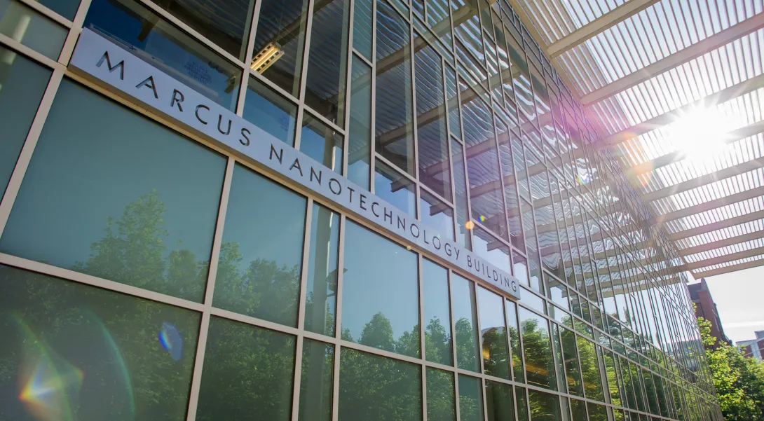
Through the Institute of Matter and Systems’ core facilities, housed in the Marcus Nanotechnology Building, DISC will accelerate semiconductor and advanced packaging development.
“The awarding of the Digital Twin Manufacturing USA Institute is a culmination of more than three years of work with the Semiconductor Research Corporation and other valued team members who share a similar vision of advancing U.S. leadership in semiconductors and advanced packaging,” said George White, senior director for strategic partnerships at Georgia Tech.
“As a founding member of the SMART USA Institute, Georgia Tech values this long-standing partnership. Its industry and academic partners, including the HBCU CHIPS Network, stand ready to make significant contributions to realize the goals and objectives of the SMART USA Institute,” White added.
Georgia Tech also plans to capitalize on the supply chain and optimization strengths of the No. 1-ranked H. Milton Stewart School of Industrial and Systems Engineering (ISyE). ISyE experts will help develop supply-chain digital twins to optimize and streamline manufacturing and operational efficiencies.
David Henshall, SRC vice president of Business Development, said, “The SMART USA Institute will advance American digital twin technology and apply it to the full semiconductor supply chain, enabling rapid process optimization, predictive maintenance, and agile responses to chips supply chain disruptions. These efforts will strengthen U.S. global competitiveness, ensuring our country reaps the rewards of American innovation at scale.”
News Contact
Amelia Neumeister | Research Communications Program Manager
Sep. 03, 2024
The Institute for Matter and Systems (IMS) has received $700,000 in funding from the National Science Foundation (NSF) for two education and outreach programs.
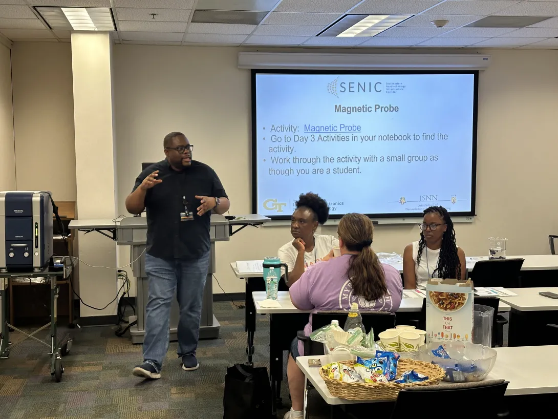
The awards will support the Research Experience for Undergraduates (REU) and Research Experience for Teachers (RET) programs at Georgia Tech. The REU summer internship program provides undergraduate students from two- and four-year programs the chance to perform cutting-edge research at the forefront of nanoscale science and engineering. The RET program for high school teachers and technical college faculty offers a paid opportunity to experience the excitement of nanotechnology research and to share this experience in their classrooms.
“This NSF funding allows us to be able to do more with the programs,” said Mikkel Thomas, associate director for education and outreach. “These are programs that have existed in the past, but we haven’t had external funding for the last three years. The NSF support allows us to do more — bring more students into the program or increase the RET stipends.”
In addition to the REU and RET programs, IMS offers short courses and workshops focused on professional development, instructional labs for undergraduate and graduate students, a certificate for veterans in microelectronics and nano-manufacturing, and community engagement activities such as the Atlanta Science Festival.
News Contact
Amelia Neumeister | Communications Program Manager
Aug. 30, 2024

W. Hong Yeo is leading a $3 million NSF research training program to develop a new generation of engineers focused on creating sustainable medical devices.
Georgia Tech researcher W. Hong Yeo has been awarded a $3 million grant to help develop a new generation of engineers and scientists in the field of sustainable medical devices.
“The workforce that will emerge from this program will tackle a global challenge through sustainable innovations in device design and manufacturing,” said Yeo, Woodruff Faculty Fellow and associate professor in the George W. Woodruff School of Mechanical Engineering and the Wallace H. Coulter Department of Biomedical Engineering at Georgia Tech and Emory University.
The funding, from the National Science Foundation (NSF) Research Training (NRT) program, will address the environmental impacts resulting from the mass production of medical devices, including the increase in material waste and greenhouse gas emissions.
Under Yeo’s leadership, the Georgia Tech team comprises multidisciplinary faculty: Andrés García (bioengineering), HyunJoo Oh (industrial design and interactive computing), Lewis Wheaton (biology), and Josiah Hester (sustainable computing). Together, they’ll train 100 graduate students, including 25 NSF-funded trainees, who will develop reuseable, reliable medical devices for a range of uses.
“We plan to educate students on how to develop medical devices using biocompatible and biodegradable materials and green manufacturing processes using low-cost printing technologies,” said Yeo. “These wearable and implantable devices will enhance disease diagnosis, therapeutics, rehabilitation, and health monitoring.”
Students in the program will be challenged by a comprehensive, multidisciplinary curriculum, with deep dives into bioengineering, public policy, physiology, industrial design, interactive computing, and medicine. And they’ll get real-world experience through collaborations with clinicians and medical product developers, working to create devices that meet the needs of patients and care providers.
The Georgia Tech NRT program aims to attract students from various backgrounds, fostering a diverse, inclusive environment in the classroom — and ultimately in the workforce.
The program will also introduce a new Ph.D. concentration in smart medical devices as part of Georgia Tech's bioengineering program, and a new M.S. program in the sustainable development of medical devices. Yeo also envisions an academic impact that extends beyond the Tech campus.
“Collectively, this NRT program's curriculum, combining methods from multiple domains, will help establish best practices in many higher education institutions for developing reliable and personalized medical devices for healthcare,” he said. “We’d like to broaden students' perspectives, move past the current technology-first mindset, and reflect the needs of patients and healthcare providers through sustainable technological solutions.”
News Contact
Jerry Grillo
Aug. 28, 2024
The National Science Foundation has awarded $2 million to Clark Atlanta University in partnership with the HBCU CHIPS Network, a collaborative effort involving historically black colleges and universities (HBCUs), government agencies, academia, and industry that will serve as a national resource for semiconductor research and education.
“This is an exciting time for the HBCU CHIPS Network,” said George White, senior director for Strategic Partnerships at Georgia Tech. “This funding, and the support of Georgia Tech Executive Vice President for Research Chaouki Abdallah, is integral for the successful launch of the CHIPS Network.”
The HBCU Chips Network works to cultivate a diverse and skilled workforce that supports the national semiconductor industry. The student research and internship opportunities along with the development of specialized curricula in semiconductor design, fabrication, and related fields will expand the microelectronics workforce. As part of the network, Georgia Tech will optimize the packaging of chips into systems.
News Contact
Georgia Tech Contact:
Amelia Neumeister | Research Communications Program Manager
Clark Atlanta University Contact:
Frances Williams
May. 07, 2024
Semiconductors make our world run, but the industry faces a turning point. For decades, computer chip efficiency has doubled every two years, but that progress is slowing. To complicate the problem further, global demand for semiconductors threatens to outpace the supply. The U.S. has the opportunity to meet the growing need for chips — both by increasing domestic manufacturing and building up the workforce, which is at its lowest in decades. To bolster semiconductor research and manufacturing, in 2022, Congress passed the $52.7 billion bipartisan CHIPS and Science Act that President Joe Biden signed into law. New paradigms and pioneers are needed to make these critical advances.
Georgia Tech is playing a significant role in creating the next generation of chips, as the Institute is especially well positioned to innovate in the semiconductor field. All areas of the semiconductor stack — the components that build a chip, from hardware to artificial intelligence — are studied at Tech, and collaboration among faculty is a hallmark of its research enterprise. Such cooperation is necessary to build better chips, since they need to be reinvented in every layer of the stack.
News Contact
Media Contact: Tess Malone | tess.malone@gatech.edu
May. 29, 2024
Georgia Tech has been selected as one of six universities globally to receive funding for the newly established Global Industrial Technology Cooperation Center. The announcement was made by the Ministry of Trade, Industry, and Energy in South Korea during the Global Open Innovation Strategy Meeting in April.
The KIAT-Georgia Tech Semiconductor Electronics Center will receive $1.8 million to establish a sustainable semiconductor electronics research partnership between Korean companies, researchers, and Georgia Tech.
“I am thrilled to announce that we have secured funding to launch a groundbreaking collaboration between Georgia Tech’s world-class researchers and Korean companies,” said Hong Yeo, associate professor and Woodruff Faculty Fellow in the George W. Woodruff School of Mechanical Engineering and the Wallace H. Coulter Department of Biomedical Engineering. “This initiative will drive the development of cutting-edge technologies to advance semiconductor, sensors, and electronics research.”
Yeo will lead the center, and Michael Filler, interim executive director for the Institute of Electronics and Nanotechnology, and Muhannad Bakir, director of the 3D Advanced Packaging Research Center, will serve as co-PIs.
The center will focus on advancing semiconductor research, a critical area of technology that forms the backbone of modern electronics.
The Cooperation Center is a global technology collaboration platform designed to facilitate international joint research and development planning, partner matching, and local support for domestic researchers. The selection of Georgia Tech underscores the Institute’s leadership and expertise in the field of semiconductors.
News Contact
Amelia Neumeister
Research Communications Program Manager