May. 14, 2026
Sleep-related breathing disorders, including sleep apnea, affect millions of people worldwide but frequently go undiagnosed. One major barrier to diagnosis is the test itself.
Traditional sleep monitoring systems often rely on bulky equipment and nasal cannulas — small tubes inserted into the nostrils to measure airflow. While effective, these systems can be uncomfortable, intrusive, and difficult to tolerate overnight, limiting their use for long-term monitoring at home.
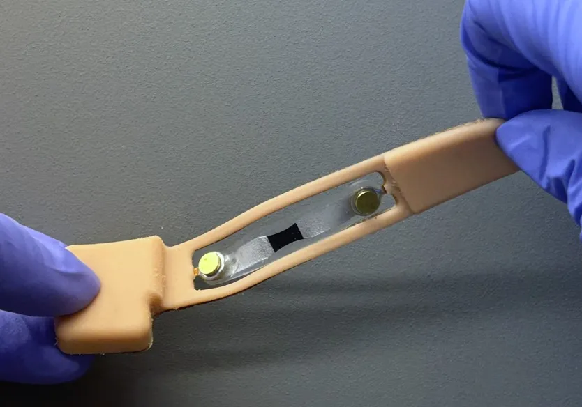
Now, researchers led by W. Hong Yeo, Peterson Professor in Pediatric Research at the George W. Woodruff School of Mechanical Engineering, have developed a soft, wireless nasal patch that could offer a more comfortable alternative for monitoring breathing during sleep.
The technology, described in a recent study published in Proceedings of the National Academy of Sciences (PNAS), uses ultrathin, skin-like wearable electronics to detect subtle movements of the nose caused by breathing without tubes, wires, or direct airflow measurements.
Read the full story on the George W. Woodruff School of Mechanical Engineering website.
News Contact
Ashley Ritchie
George W. Woodruff School of Mechanical Engineering
May. 05, 2026
The most unassuming actions can have the greatest outcomes. For Brandon Harrington, CmpE 2005, M.S. CmpE 2008, walking through the doors of the Pettit Microelectronics Building, then home to the Microelectronics Research Center (MiRC), during his freshman year 25 years ago changed the course of his career.
Each week on his way to the Howey Physics Building, Harrington passed the MiRC, wondering what happened behind its doors.
“One day I got the courage to walk in. I went to the front desk and I asked, ‘Hey, do you have any jobs for freshmen?’” Harrington recalled. “I was pointed to Bob Rose, so I walked down and had a brief conversation with him where he hired me on the spot.”
That moment—walking in with curiosity and leaving with a job— shifted Harrington’s career path from pursuing a bachelor’s degree in computer engineering and working in electronic design automation (EDA) to a life in the laboratory advancing microelectronics research.
When he began working for the MiRC in the early 2000s, the cleanroom facilities had only three full-time employees. The small staff gave Harrington opportunities to contribute. He started with smaller tasks, from changing pump oil to sorting nuts and bolts, but his dedication quickly led to greater responsibility.
At the time, Gary Spinner, director of cleanroom operations for the Institute for Matter and Systems (IMS), played a key role in mentoring students and expanding access to the Institute’s microelectronics facilities. Known for his hands-on approach and commitment to student development, Spinner helped guide the growth of cleanroom operations and the people who worked within them.
“Gary took note of me and said, ‘Brandon, please join the co-op program,’” Harrington said. “I quickly found my way into the cleanrooms, and from that point on, I touched basically every system, whether it was the billing software, the access control system, or the toxic gas monitoring.”
As an undergraduate co-op, Harrington advanced through the MiRC, training graduate researchers on tools and developing new or modifying existing efficiency systems. By the time he earned his undergraduate degree, he had accumulated extensive experience in the cleanrooms and graduated with an offer to be a full-time electrical engineer for the MiRC while pursuing his master’s degree.
An unexpected outcome of this role was a friendship that led him to a Ph.D. in electrical engineering. While working full-time, Harrington became good friends with then-Ph.D. student Reza Abdolvand. After Abdolvand joined Oklahoma State University as a faculty member, he asked Harrington if he would come help him start his research group.
“I was really good friends with Reza and I thought this was a way I could get his career going,” Harrington said. “So I left Georgia Tech, around 2008, to pursue my PhD from Oklahoma State.”
Today, Harrington supports the industry in a variety of ways, providing consultation for startups and large corporations alike. His work includes early feasibility studies, prototype development, productization, transfer to volume-production foundries, and yield improvement activities.
He is now the director of microelectromechanical systems (MEMS) development at AMFitzgerald, where he leads a team delivering innovative solutions to clients—all because he followed his curiosity.
Harrington’s journey reflects the broader impact of Georgia Tech’s cleanroom facilities—spaces where curiosity can turn into hands-on experience, mentorship, and career-defining opportunities. By providing students access to advanced tools, real-world problem-solving, and a collaborative research environment, the cleanrooms continue to shape the next generation of engineers and innovators, just as they did for a curious freshman who decided to walk through an open door.
News Contact
Writer: Gabriel Buggi | Communications Student Assistant
Media Contact: Amelia Neumeister | Communications Manager
The Institute for Matter and Systems
Mar. 27, 2026

Eric Vogel welcomed attendees to Energy Day.
 with Amit Kulkarni (center) and Jim Walsh (right), both speakers from GE Vernova.</p>")
Georgia Tech EVPR Tim Lieuwen (left) with Amit Kulkarni (center) and Jim Walsh (right), both speakers from GE Vernova.

Marta Hatzell served as Energy Day emcee.

Vanessa Chan gave the keynote presentation at Energy Day.
 moderated the Beyond Scarcity: Building Resilient Critical Materials Supply Chains for Energy Systems panel.</p>")
Yaunzhi Tang (left) moderated the Beyond Scarcity: Building Resilient Critical Materials Supply Chains for Energy Systems panel.

Students participated in the Energy Day poster session.
More than 300 leaders from industry, government, and academia gathered on Georgia Tech’s campus for Energy Day, a one-day conference focused on one of today’s most urgent challenges: meeting the rapidly growing energy demands of artificial intelligence (AI).
Held on March 19, the event was co-hosted by Georgia Tech’s Institute for Matter and Systems (IMS) and Strategic Energy Institute (SEI) with plenary support from the Energy Policy and Innovation Center. This year’s theme, Energy for AI, anchored discussions on how energy systems must evolve to support an increasingly digital and computer-intensive world.
“Energy Day demonstrates how critical it is to align research, industry, and policy to manage rising power demand and modernize our energy systems,” said Yuanzhi Tang, SEI’s executive director. “At Georgia Tech, we are committed to advancing solutions that translate research into impact at the speed innovation demands.”
This year’s Energy Day continued the momentum of past events, beginning with Battery Day in 2023. As research priorities have expanded, the event has grown to highlight Georgia Tech and the state of Georgia as national hubs for next-generation energy innovation, advanced manufacturing, and data-driven infrastructure.
The program was structured to foster high-level dialogue through keynote presentations and panel discussions, as well as deeper, focused tracks on specialized technical topics. The morning session featured a fireside chat between presenting sponsor GE Vernova and Georgia Tech Executive Vice President for Research Tim Lieuwen, followed by a keynote address from Vanessa Chan, former U.S. Department of Energy official and expert in commercialization and innovation, and two panels focused on policy, materials, and the evolving energy ecosystem.
“Great ideas usually come out when you bring together different perspectives,” said Eric Vogel, executive director of IMS. “That’s why we have this event. It helps scientists think more broadly, connects policymakers to science, and demonstrates the strength of Georgia Tech’s research community.”
In the afternoon, attendees split into three technical tracks addressing critical challenges at the intersection of energy and AI — from power delivery and storage to materials, infrastructure, and system resilience.
Designed to bring together researchers, policy makers, industry leaders, and students, Energy Day continues to drive interdisciplinary collaboration. Conversations throughout the day centered on three ideas: the magnitude and certainty of rising global energy demand, the urgency of scaling solutions efficiently, and the necessity of broad collaboration across research, industry, policy, and workforce pathways.
The event concluded with a student poster session featuring more than 20 research presentations, highlighting emerging work from across Georgia Tech. Three were recognized for excellence:
First place: Douglas Nelson — Improving Energy Efficiency in Fume Hoods and Ultra-Low Temperature Freezers
Finalist: Erik Barbosa — Multiscale Approach for Thermochemical Energy Storage in Buildings
Finalist: Ricardo Cruzado Valladares — Energy-Water Nexus for Sustainable AI Data Centers
Mar. 12, 2026

Since 2020, Georgia Tech has partnered with Sandia National Laboratories, a federally funded research and development center focused on national security. In February, the two institutions renewed their collaboration with a new Memorandum of Understanding (MOU), reaffirming a relationship that has already strengthened research capabilities on both sides.
The partnership has driven progress in areas ranging from hypersonics to bioscience, while also deepening institutional ties beyond research. Joint faculty appointments — such as Anirban Mazumdar, who holds roles at both Sandia and the George W. Woodruff School of Mechanical Engineering — demonstrate how closely the organizations work together. The collaboration has also expanded student talent pipelines, providing more avenues for Georgia Tech students to pursue careers at the national lab.
“At its core, this partnership is about people,” said Tim Lieuwen, executive vice president for Research at Georgia Tech. “Sandia and Georgia Tech share a commitment to discovery and developing the talent, creativity, and collaboration our nation needs.”
The renewed MOU, he said, “strengthens connections between our researchers, opens new doors for our students, and builds meaningful career pathways into national service. When our communities work together to address national priorities, we not only accelerate technological advances — we expand opportunities for the people who will shape the future of our nation’s security.”
Under the new MOU, Sandia and Georgia Tech will focus on integrated research across key national security‑aligned areas, including secure artificial intelligence and computing, quantum technologies, critical minerals, advanced manufacturing, energy and grid resilience, and hypersonics. The partnership emphasizes connecting manufacturing, computation, and systems approaches directly to national security applications.
“Together, we have been solving new and unprecedented challenges in science and engineering, and now we have a great opportunity to develop this partnership,” said Dan Sinars, Sandia’s deputy chief research officer. “Our research benefits both national security and national prosperity, and keeps the country at the forefront of the world.”
With this strengthened connection, the partners aim to grow their shared research footprint through increased funding, publications, and faculty-led startups. Over the long term, Georgia Tech intends to become one of Sandia’s top hiring pipelines, ensuring that talent developed through joint research continues into national security careers.
History of the Partnership
The Institute’s collaboration with Sandia began in the mid‑2010s, when the labs selected Georgia Tech as one of its partner institutions. The first MOU, signed in 2015, formalized the relationship and outlined initial technical focus areas.
In 2018, George White, executive director of strategic partnerships, and Olof Westerstahl, senior director strategic initiatives in the Office of Corporate Engagement, helped expand the partnership. They launched “Sandia Day,” an event designed to introduce Georgia Tech faculty to Sandia researchers and spark new collaborations. By 2020, the organizations signed a second MOU that expanded the partnership’s technical focus areas to include energy and grid security, materials and nanotechnology, advanced electronics, advanced manufacturing, advanced computing, cyber and information security, bioscience, hypersonics, quantum information science, and engineering sciences.
The results have been substantial. Since 2018, Sandia has sponsored $35 million in research collaborations with Georgia Tech. Researchers from both institutions have co-authored 450 publications since 2016. Research activity continues to accelerate, with $1.6 million in new contracts in the past year alone. As of August 2025, Sandia employs 325 Georgia Tech alumni — a testament to the impact of the growing talent pipeline.
“We view our work with Sandia as the model for engagement with other national labs,” said White. “With the new MOU, we will continue to grow the Sandia partnership. I would like to see our footprint double in scope in the next five years.”
News Contact
Tess Malone, Senior Research Writer/Editor
tess.malone@gatech.edu
Feb. 20, 2026

While Italy’s 2026 Winter Olympics draw the world’s attention to snow and ice, Georgia Tech researchers are also confronting cold at its most extreme.
Some labs in the School of Electrical and Computer Engineering (ECE) use liquid nitrogen and liquid helium to chill cryogenic test systems to as low as 4 Kelvins (K), or -452.47 degrees Fahrenheit (F), temperatures that rival the coldest regions of deep space.
At this point, materials and electronic devices stop behaving in familiar ways, which is exactly why ECE researchers use these extreme conditions to explore and develop new semiconductor technologies.
“Electronics are very temperature dependent,” Professor John Cressler said, whose lab houses some of these cryogenic test systems. “Whether you see it or not, every electronic you buy has a tested temperature spec associated with it.”
Current commercially sold devices, including most cell phones, are made to run between 32 F and 85 F. Researchers in ECE test across a far wider range, as they develop technology with extraterrestrial and quantum computing applications in mind.
Other ECE teams work in natural extremes, carrying instruments into polar regions where cold creates challenges that no lab can fully replicate.
Just as cold pushes athletes in different ways, it guides ECE research down its own distinct paths.
Read the full story on the School of Electrical and Computer Engineering's website.
News Contact
Zachary Winiecki
Feb. 18, 2026

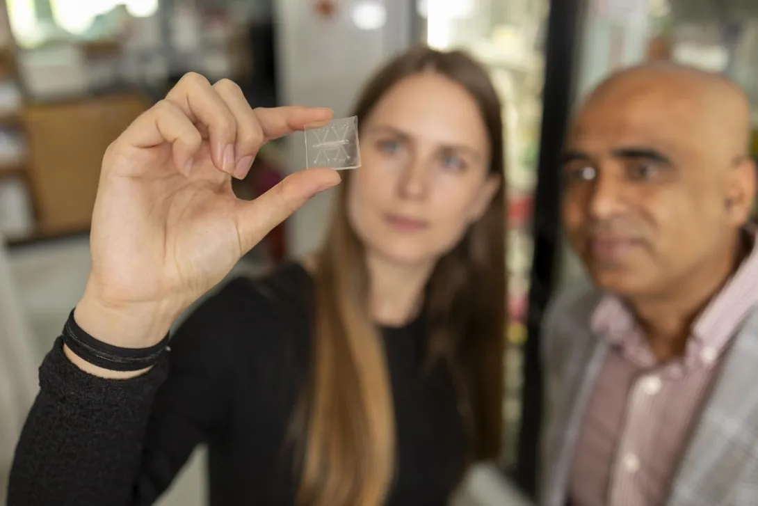
GTRI and Georgia Tech's smart bandage could revolutionize wound care by enabling real-time insights on healing and reducing invasive bandage changes.
While most people don’t think twice about a cut or scrape, for those with diabetes, every wound is a potential threat that requires vigilant care.
Diabetic foot ulcers, for example, are slow to heal and can increase the risk of infection, hospitalization, and even amputation.
To address this critical challenge, researchers at the Georgia Institute of Technology (Georgia Tech) and the Georgia Tech Research Institute (GTRI) have developed a sensor designed to monitor chronic wounds in real-time. Embedded directly into a bandage, this flexible, low-cost device could transform wound management for diabetic patients and other critical applications — such as providing direct treatment to soldiers on the battlefield or managing chronic wounds in elderly populations and patients with limited healthcare access — by reducing invasive bandage changes and ensuring timely medical intervention.
“For diabetic patients with foot ulcers, long-term monitoring and care are essential,” said GTRI Principal Research Engineer and Project Lead Judy Song. “We were inspired by the success of wearable glucose monitors to develop a compact, affordable sensor tailored to wound care.”
This project was supported by GTRI’s Independent Research and Development (IRAD) program between 2022-2025 and reflects the strength of interdisciplinary collaboration across Georgia Tech. Researchers from three out of GTRI’s eight laboratories developed the sensor with experts from the George W. Woodruff School of Mechanical Engineering, the H. Milton Stewart School of Industrial and Systems Engineering and the Wallace H. Coulter Department of Biomedical Engineering at Tech and Emory University.
About one in four people with diabetes will develop a foot ulcer at some point in their lives, making it one of the leading causes of foot amputations. For these patients, nerve damage and poor blood flow hinder the body’s natural healing process and allow wounds to linger and worsen.
During the initial phases of their research, the team noted that nitric oxide (NO) had been previously identified as a key biomarker for wound health due to its central role in the healing process. Nitric oxide improves blood flow, reduces inflammation, promotes tissue growth and fights infection. By tracking nitric oxide levels in wounds, clinicians could determine whether a wound is improving or detect early signs of trouble.
"Nitric oxide plays a fascinating, almost paradoxical, role in wound healing,” said GTRI Senior Research Engineer Victoria Razin, who is co-leading the project. “It’s essential for processes like blood flow and tissue repair, but can also signal when something is going wrong.”
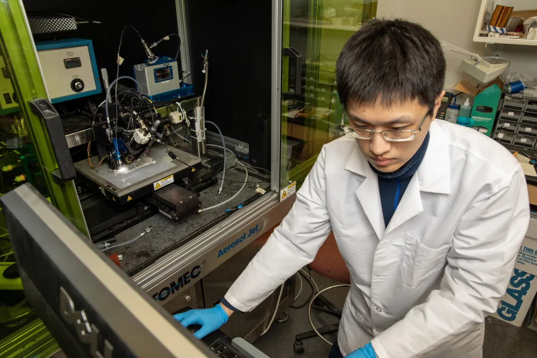
At the core of the smart bandage is a flexible sensor powered by a three-electrode system capable of detecting changes in nitric oxide. The team used advanced Aerosol Jet® printing techniques to fabricate the sensor, significantly reducing production costs from thousands of dollars to just a few dollars per unit and making the design more affordable and scalable.
“Typically, prototyping these sensors can cost thousands of dollars, but our approach brought costs down dramatically,” said Chuck Zhang, the Eugene C. Gwaltney, Jr. Chair and Professor in ISYE and a program director at the National Science Foundation (NSF), who oversaw sensor fabrication for this project. “Lower costs let us iterate quickly and deliver something that could have real healthcare impact.”
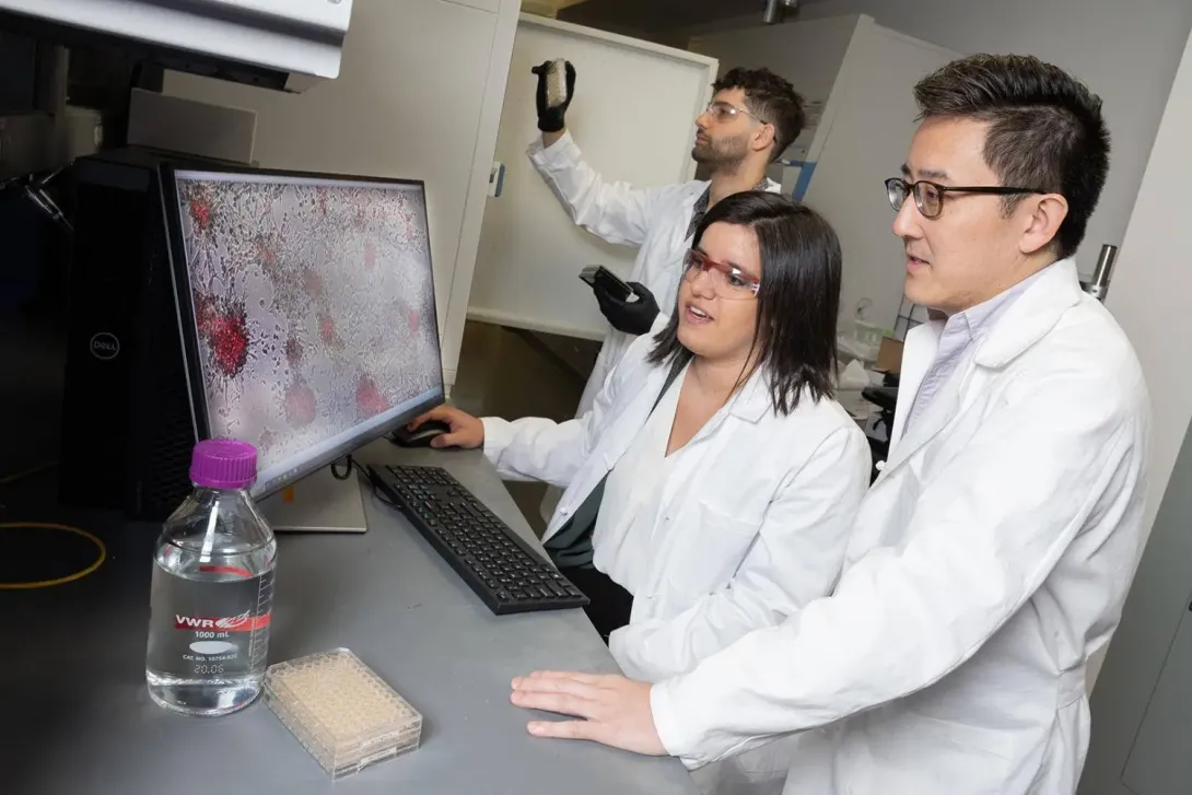
To test the sensor’s accuracy, the team conducted extensive laboratory studies in both biological and simulated wound conditions.
In one set of experiments, endothelial cell cultures were used to create “wounds” by scraping the cell layers. As the cells migrated to repair the gap, nitric oxide production increased, and the sensor successfully tracked these changes in real-time. Additional fluid tests using blood plasma and red blood cells demonstrated that the sensor could reliably detect nitric oxide in a variety of conditions that closely mimic real-world wound environments.
These experiments confirmed that the sensor can identify the fluctuations in nitric oxide associated with different phases of wound healing.
Lab testing was led by Dr. Wilbur Lam, a professor in the Department of Biomedical Engineering and at Emory University School of Medicine, with support from Kirby Fibben, a biomedical engineering Ph.D. student at Tech.
"There’s a significant clinical need for real time, minimally invasive sensor technologies that detect nitric oxide,” said Dr. Lam. “While we’re starting with wound healing, there’s multiple other applications for vascular, hematologic, and pulmonary diseases as well.”
The next step in the project is integrating the sensor into a functional wearable device. The team is combining the sensor with a miniaturized potentiostat (MicroPS) – a small electronic device that measures chemical signals – along with flexible electronic components and a system to transmit data to a mobile app.
The MicroPS, designed by the GTRI research team, led by GTRI Research Engineer Curtis Mulady, enables compact electrochemical measurements and the wireless platform transmits nitric oxide readings from the bandage to a mobile app via Bluetooth. The app uploads the data to a cloud platform, giving clinicians the ability to remotely monitor wound progress in real time. This system could reduce the need for frequent in-person checkups, enabling earlier interventions and improving outcomes for patients.
Future iterations of the bandage aim to include “closed-loop” systems capable of both monitoring and treating wounds, said GTRI’s Song. For example, sensors could trigger a response, like releasing therapeutic agents or antimicrobials directly to the wound, when abnormalities are detected.
The researchers are also exploring commercialization pathways, including partnerships with medical device companies or the formation of a startup.
“This sensor meets a real need for early detection of infection and to evaluate wound healing, and I believe it could have significant commercial success,” said Peter Hesketh, a professor in the School of Mechanical Engineering who led sensor design and performance testing.
Other contributors to this project from GTRI include Mulady, Cora Weidner, Maxwell Blanchard, Rachel Erbrick and Christopher Heist. Zhaonan “Zeke” Liu, a postdoctoral fellow in ISYE, assisted with sensor fabrication, while Rizky Ilhamsyah, a graduate research assistant in the School of Mechanical Engineering, contributed to sensor design and performance testing.
Writer: Anna Akins
Photos: Sean McNeil
GTRI Communications
Georgia Tech Research Institute
Atlanta, Georgia USA
For more information, please contact gtri.media@gtri.gatech.edu.
To learn more about GTRI, visit: Georgia Tech Research Institute | GTRI
News Contact
For more information, please contact gtri.media@gtri.gatech.edu
Writer: Anna Akins (anna.akins@gtri.gatech.edu).
Jan. 05, 2026
University research drives U.S. innovation, and Georgia Institute of Technology is leading the way.
The latest Higher Education Research and Development (HERD) Survey from the National Science Foundation (NSF) places Georgia Tech as No. 2 nationally for federally sponsored research expenditures in 2024. This is Georgia Tech’s highest-ever ranking from the NSF HERD survey and a 70% increase over the Institute's 2019 numbers.
In total expenditures from all externally funded dollars (including the federal government, foundations, industry, etc.), Georgia Tech is ranked at No. 6.
Tech remains ranked No. 1 among universities without a medical school — a major accomplishment, as medical schools account for a quarter of all research expenditures nationally.
“Georgia Tech’s rise to No. 2 in federally sponsored research expenditures reflects the extraordinary talent and commitment of our faculty, staff, students, and partners. This achievement demonstrates the confidence federal agencies have in our ability to deliver transformative research that addresses the nation’s most critical challenges,” said Tim Lieuwen, executive vice president for Research.
Overall, the state of Georgia maintained its No. 8 position in university research and development, and for the first time, the state topped the $4 billion mark in research expenditures. Georgia Tech provides $1.5 billion, the largest state university contribution. In the last five years, federal funding for higher education research in the state of Georgia has grown an astounding 46% — 10 points higher than the U.S. rate.
Lieuwen said, “Georgia Tech is proud to lead the state in research contributions, helping Georgia surpass the $4 billion mark for the first time. Our work doesn’t just advance knowledge — it saves lives, creates jobs, and strengthens national security. This growth reflects our commitment to drive innovation that benefits Georgia, our country, and the world.”
About the NSF HERD Survey
The NSF HERD Survey is an annual census of U.S. colleges and universities that expended at least $150,000 in separately accounted for research and development (R&D) in the fiscal year. The survey collects information on R&D expenditures by field of research and source of funds and also gathers information on types of research, expenses, and headcounts of R&D personnel.
About Georgia Tech's Research Enterprise
The research enterprise at Georgia Tech is led by the Executive Vice President for Research, Tim Lieuwen, and directs a portfolio of research, development, and sponsored activities. This includes leadership of the Georgia Tech Research Institute (GTRI), the Enterprise Innovation Institute, 11 interdisciplinary research institutes (IRIs), Office of Commercialization, Office of Corporate Engagement, plus research centers, and related research administrative support units. Georgia Tech routinely ranks among the top U.S. universities in volume of research conducted.
News Contact
Angela Ayers
Assistant Vice President of Research Communications
Georgia Tech
Nov. 20, 2025
Georgia Institute of Technology has been ranked 7th in the world in the 2026 Times Higher Education Interdisciplinary Science Rankings, in association with Schmidt Science Fellows. This designation underscores Georgia Tech’s leadership in research that solves global challenges.
“Interdisciplinary research is at the heart of Georgia Tech’s mission,” said Tim Lieuwen, executive vice president for Research. “Our faculty, students, and research teams work across disciplines to create transformative solutions in areas such as healthcare, energy, advanced manufacturing, and artificial intelligence. This ranking reflects the strength of our collaborative culture and the impact of our research on society.”
As a top R1 research university, Georgia Tech is shaping the future of basic and applied research by pursuing inventive solutions to the world’s most pressing problems. Whether discovering cancer treatments or developing new methods to power our communities, work at the Institute focuses on improving the human condition.
Teams from all seven Georgia Tech colleges, 11 interdisciplinary research institutes, the Georgia Tech Research Institute, Enterprise Innovation Institute, and hundreds of research labs and centers work together to transform ideas into real results.
News Contact
Angela Ayers
Sep. 18, 2025

Hong Yeo holds the wearable electronic device made of more than 170 thin, flexible sensors that measure foot pressure — a key metric for determining whether someone is off-balance. [Photos by Joya Chapman]

The wearable electronic device, developed by Georgia Tech researchers, is made of more than 170 thin, flexible sensors that measure foot pressure — a key metric for determining whether someone is off-balance.
Maintaining balance while walking may seem automatic — until suddenly it isn’t. Gait impairment, or difficulty with walking, is a major liability for stroke and Parkinson’s patients. Not only do gait issues slow a person down, but they are also one of the top causes of falls. And solutions are often limited to time-intensive and costly physical therapy.
A new wearable electronic device that can be inserted inside any shoe may be able to address this challenge. The device, developed by Georgia Tech researchers, is made of more than 170 thin, flexible sensors that measure foot pressure — a key metric for determining whether someone is off-balance. The sensor collects pressure data, which the researchers could eventually use to predict which changes lead to falls.
The researchers presented their work in the paper, “Flexible Smart Insole and Plantar Pressure Monitoring Using Screen-Printed Nanomaterials and Piezoresistive Sensors.” It was the cover paper in the August edition of ACSApplied Materials & Interfaces.
Pressure Points
Smart footwear isn’t new — but making it both functional and affordable has been nearly impossible. W. Hong Yeo’s lab has made its reputation on creating malleable medical devices. The researchers rely on the common commercial practice of screen-printing electronics to screen-print sensors. They realized they could apply this printing technique to address walking difficulties.
“Screen-printing is advantageous for developing medical devices because it's low-cost and scalable,” said Yeo, the Peterson Professor and Harris Saunders Jr. Professor in the George W. Woodruff School of Mechanical Engineering. “So, when it comes to thinking about commercialization and mass production, screen-printing is a really good platform because it's already been used in the electronics industry.”
Making the device accessible to the everyday user was paramount for Yeo’s team. A key innovation was making sure the wearable is thin enough to be comfortable for the wearer and easy to integrate with other assistive technologies. The device uses Bluetooth, enabling a smartphone to collect data and offer the future possibility of integrating with existing health monitoring applications.
Possibilities for real-world adaptation are promising, thanks to these innovations. Lightweight and small, the wearable could be paired with robotics devices to help stroke and Parkinson’s patients and the elderly walk. The high number of sensors could make it easier for researchers to apply a machine learning algorithm that could predict falls. The device could even enable professional athletes to analyze their performance.
Regardless of how the device is used, Yeo intends to keep its cost under $100. So far, with funding from the National Science Foundation, the researchers have tested the device on healthy subjects. They hope to expand the study to people with gait impairments and, eventually, make the device commercially available.
“I'm trying to bridge the gap between the lack of available devices in hospitals or medical practices and the lab-scale devices,” Yeo said. “We want these devices to be ready now — not in 10 years.”
With its low-cost, wireless design and potential for real-time feedback, this smart insole could transform how we monitor and manage walking difficulties — not just in clinical settings, but in everyday life.
News Contact
Tess Malone, Senior Research Writer/Editor
tess.malone@gatech.edu
Aug. 07, 2025

Nazanin Bassiri-Gharb, Harris Saunders, Jr. Chair and Professor in the Woodruff School and MSE, and Yao Xie, Coca-Cola Foundation Chair and Professor in ISyE.
In the world of nanotechnology, seeing clearly isn’t easy. It’s even harder when you’re trying to understand how a material’s properties relate to its structure at the nanoscale. Tools like piezoresponse force microscopy (PFM) help scientists peer into the nanoscale functionality of materials, revealing how they respond to electric fields. But those signals are often buried in noise, especially in instances where the most interesting physics happens.
Now, researchers at Georgia Tech have developed a powerful new method to extract meaningful information from even the noisiest data, or when, alternatively, the response of the material is the smallest. Their approach, which combines physical modeling with advanced statistical reconstruction, could significantly improve the accuracy and confidence of nanoscale measurement properties.
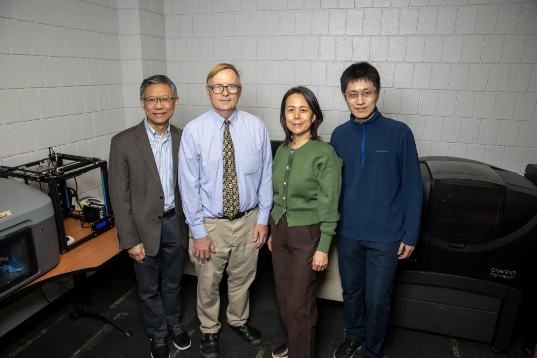
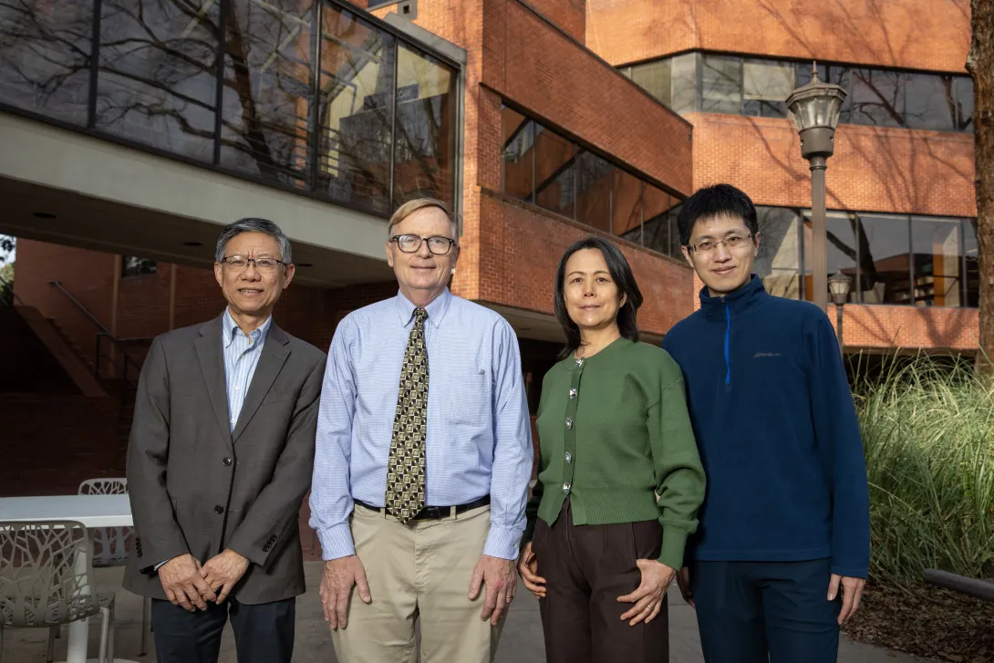
The team’s findings, led by Nazanin Bassiri-Gharb, Harris Saunders, Jr. Chair and Professor in the George W. Woodruff School of Mechanical Engineering and School of Materials Science and Engineering (MSE), are reported in Small Methods.
Co-lead authors Kerisha Williams, a former MSE Ph.D. student, and Henry Shaowu Yuchi, a former Ph.D. student in the H. Milton Stewart School of Industrial and Systems Engineering (ISyE), spearheaded the study. Other collaborators include Kevin Ligonde, a Ph.D. student in the Woodruff School; Mathew Repasky, a former Ph.D. student in ISyE; and Yao Xie, Coca-Cola Foundation Chair and Professor in ISyE.
This research was initiated through Georgia Tech’s Forming Teams and Moving Teams Forward seed grant program, launched by the Office of the Executive Vice President for Research in 2021. Designed to support cross-disciplinary collaboration, the program helps build research teams that align with the growing national emphasis on large-scale, team-based projects. The grant supported early work by Bassiri-Gharb, Xie, and Juan-Pablo Correa-Baena, associate professor and Goizueta Early Career Faculty Chair in MSE.
Read the full story on the George W. Woodruff School of Mechanical Engineering website.
News Contact
Ashley Ritchie
George W. Woodruff School of Mechanical Engineering