Jun. 27, 2025

The Institute for Matter and Systems is proud to announce the recipients of the IMS Employee Excellence Awards, recognizing five outstanding individuals for their exceptional contributions to the IMS community. These awards honor staff and research faculty who have gone above and beyond their regular responsibilities to advance IMS’s mission and values.
More than 40 nominations were submitted, representing over 20 employees for their work during the 2024-2025 fiscal year. Nominators included IMS staff, facility users, center directors, and affiliated faculty.
Each recipient was recognized at the IMS Summer Staff Event held in June 2025.
Meet the Employees of Excellence:
Hang Chen– Cleanroom Process and Instructional Support Manger
Hang Chen was recognized for his dedication and adaptability in taking on a significantly expanded workload following a key staff departure—all while continuing to lead the cleanroom process support team and manage multiple projects. His efforts directly contributed to record-breaking external user engagement and revenue, demonstrating his impact on Georgia Tech’s research infrastructure. Hang’s willingness to go above and beyond exemplifies the spirit of excellence and service.
Yong Ding – Principal Research Engineer
Yong Ding was honored for his exceptional leadership, technical mastery in electron microscopy, and unwavering dedication to mentoring students and researchers at Georgia Tech. Across multiple nominations, he was praised for making complex microscopy techniques accessible, maintaining cutting-edge instrumentation through strong industry partnerships, and fostering a collaborative, inclusive learning environment. His impact extends far beyond his formal duties—advancing research, empowering the next generation of scientists, and ensuring the electron microscopy facility remains a world-class resource.
Rebecca Grieco – Events/Marketing Coordinator
Rebecca Grieco was celebrated for her leadership in event planning and outreach, having flawlessly managed more than 50 events and consistently ensured a welcoming, professional experience for all guests. Her initiative, attention to detail, and commitment to promoting IMS programs have significantly enhanced the institute’s visibility and engagement across campus. Rebecca’s reliability and dedication make her a standout contributor to the IMS community.
Gary Spinner – Associate Director of Cleanroom and Fabrication Facilities
Gary Spinner was honored for his leadership and technical expertise in managing Georgia Tech’s Marcus and Pettit microfabrication cleanrooms—critical facilities for cutting-edge research. His ability to balance complex technical operations with compassionate, effective team management has made the cleanroom a model of excellence. Gary’s dedication to education, outreach, and workforce development has also had a lasting impact on students and the broader research community.
Weston Straka – Research Scientist II
Weston Straka was recognized for his leadership and technical skill in supporting the Mechanical Properties Research Facility during a period of major disruption. He stabilized operations, led critical equipment repairs, supported students, and coordinated the search for a permanent facility lead—all while continuing to train and assist hundreds of researchers across multiple MCF tools. His ability to manage crisis while excelling in his core responsibilities exemplifies outstanding service and dedication.
These individuals embody the spirit of excellence, innovation, and service that defines IMS. Their work has had a lasting impact on our research community and beyond.
News Contact
Amelia Neumeister | Research Communications Program Manager
The Institute for Matter and Systems
Jun. 24, 2025
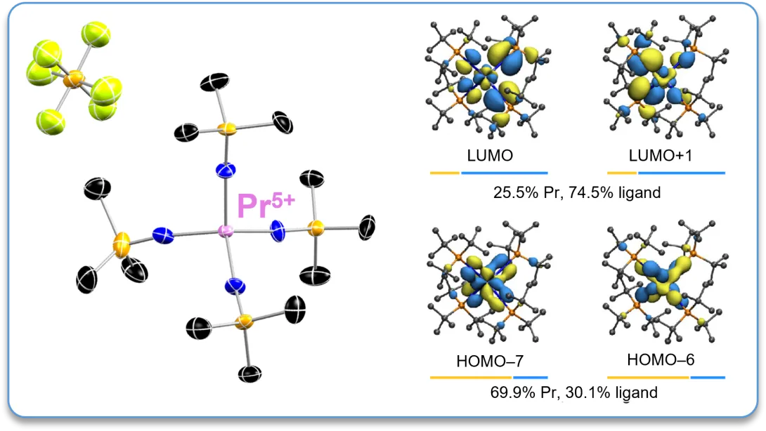
A longstanding mystery of the periodic table involves a group of unique elements called lanthanides. Also known as rare earth elements, or REEs, these silvery-white metals are challenging to isolate, given their very similar chemical and physical properties. This similarity makes it difficult to distinguish REEs from one other during extraction and purification processes.
The world has come to depend on lanthanides’ magnetic and optical properties to drive much of modern technology — from medical imaging to missiles to smart phones. These metals also are in short supply, and because they’re found in minerals, lanthanides are difficult to mine and separate. But that may change — thanks to a Georgia Tech-led discovery of a new oxidation state for a lanthanide element known as praseodymium.
For the first time ever, praseodymium achieved a 5+ oxidation state. Oxidation occurs when a substance meets oxygen or another oxidizing substance. (The browning on the flesh of a cut apple, as well as rust on metal, are examples of oxidation.)
As far back as the 1890s, scientists suspected lanthanides might have a 5+ oxidation state, but lanthanides in that state were too unstable to see, said Henry ”Pete“ La Pierre, an associate professor in Georgia Tech’s School of Chemistry and Biochemistry. Discovering an element’s new oxidation state is like discovering a new element. As an example, La Pierre noted how plutonium’s discovery opened up a whole new area of the periodic table.
“A new oxidation state tells us what we don’t know and gives us ideas for where to go,” he explained. “Each oxidation state of an element has distinct chemical and physical properties — so the first glimpse of a novel oxidation presents a roadmap for new possibilities.”
La Pierre and colleagues at University of Iowa and Washington State University recently discovered the 5+ oxidation state for lanthanides.
“It was predicted but never seen until we found it,” said La Pierre, corresponding author of the study, “Praseodymium in the Formal +5 Oxidation State,” which was recently published in Nature Chemistry. “Lanthanides’ properties are really fantastic. We only use them commercially in one oxidation state — the 3+ oxidation state — which defines a set of magnetic and optical properties. If you can stabilize a higher oxidation state, it could lead to entirely new magnetic and optical properties.”
The researchers’ breakthrough will broaden the lanthanides’ technical applications in fields such as rare-earth mining and quantum technology and could lead to new electronic device architectures and applications.
“Research in lanthanides has already yielded significant dividends for society in terms of technological development,” La Pierre added.
The researchers hope to discover new tools for mining critical REEs, including improving lanthanide separation and recycling processes. When mining these elements, lanthanide elements are frequently mixed together. The separation process is painstaking and inefficient, generating a significant amount of waste. But with increasing global demand for REEs, the U.S. faces a supply issue. Figuring out how to improve lanthanides separation, potentially through oxidation chemistry, will ultimately enhance the supply of these critical elements.
— Anne Wainscott-Sargent
Funding: This research was supported by grants from the National Science Foundation and the U.S. Department of Energy.
News Contact
Shelley Wunder-Smith
Director of Research Communications
Jun. 18, 2025
The Institute for Matter and Systems (IMS) at Georgia Tech has announced the Spring 2025 Core Facility Seed Grant recipients. The primary purpose of this program is to give graduate students in diverse disciplines working on original and unfunded research in micro- and nanoscale science and engineering the opportunity to access the most advanced academic cleanroom space in the Southeast. In addition to using the labs' state-of-the-art fabrication, lithography, and characterization tools, the awardees will have the opportunity to gain proficiency in cleanroom and tool methodology and access the consultation services provided by research staff members in IMS. Seed Grant awardees are also provided travel support to present their research at a scientific conference.
In addition to student research skill development, this biannual grant program gives faculty with novel research topics the ability to develop preliminary data to pursue follow-up funding sources. The Core Facility Seed Grant program is supported in part by the Southeastern Nanotechnology Infrastructure Corridor (SENIC), a member of the National Science Foundation’s National Nanotechnology Coordinated Infrastructure (NNCI).
The five winning projects in this round were awarded IMS cleanroom and lab access time to be used over the next year.
The Spring 2025 IMS Core Facility Seed Grant recipients are:
Stretchable Power Sources for Vertically Integrated Bioelectronics
PI: Antonio Facchetti
Student: Sakshi Sharma
School of Materials Science and Engineering
Next-generation 3D Solid-state Neutron Detectors for Nuclear Nonproliferation
PI: Anna Erickson
Student: David Straub
George W. Woodruff School of Mechanical Engineering
Programmable Microchip-based Cytotoxicity Assay for Real-Time Immune Cell Profiling
PI: Fatih Sarioglu
Student: Ahmadreza Rostamzadeh
School of Electrical and Computer Engineering
Experimental Study of Neutron-induced Radiation Damage in Lunar Materials with Key Implications for the Future of Lunar Geochronology
PI: Karl Lang
Student: Shreya Mukherjee
School of Earth and Atmospheric Sciences
Enhanced Dielectrophoretic Enrichment and Removal of Microplastics from Drinking Water via Engineered Nonuniform Electric Fields on Microfluidic Chips
PI: Xing Xie
Student: Shuai Wang
School of Civil and Environmental Engineering
News Contact
Amelia Neumeister | Research Communications Program Manager
Institute for Matter and Systems
Jun. 05, 2025

Sun Geun Yoon works in a glove box in McDowell’s laboratory at Georgia Tech. [Photo by Christopher McKenney]
Lithium-ion batteries power everything from electric cars to laptops to leaf blowers. Despite their widespread adoption, lithium-ion batteries carry limited amounts of energy, and rare overheating can lead to safety concerns. Consequently, for decades, researchers have sought a more reliable battery.
Solid-state batteries are less flammable and can hold more energy, but they often require intense pressure to function. This requirement has made them difficult to use in applications, but new research from Georgia Tech could change that.
The research group of Matthew McDowell, professor and Carter N. Paden Jr. Distinguished Chair in the George W. Woodruff School of Mechanical Engineering and the School of Materials Science and Engineering, has designed a new metal for solid-state batteries that enables operation at lower pressures. While lithium metal is often used in these batteries, McDowell’s group discovered that combining lithium with softer sodium metal results in improved performance and novel behavior.
McDowell and his collaborators presented their findings in the paper, “Interface Morphogenesis with a Deformable Secondary Phase in Solid-State Lithium Batteries,” published in Science on June 5.
Stackable Solution
Lithium-ion batteries have been the industry standard because they combine compact size, reliability, and longevity. However, they contain a liquid “electrolyte,” which helps lithium ions move in the battery but is also flammable. In solid-state batteries, this electrolyte is a solid material that is less flammable. The challenge is that when the battery is used, the lithium metal in the battery changes its shape, potentially losing contact with the solid electrolyte, which degrades performance. A common way to ensure the metal doesn’t lose contact is to apply high pressure to these batteries.
“A solid-state battery usually requires metal plates to apply this high pressure, and those plates can be bigger than the battery itself,” McDowell said. “This makes the battery too heavy and bulky to be effective.”
The researchers, led by Georgia Tech research scientist Sun Geun Yoon, sought a solution. The solid-state batteries would still require some pressure to function, but they found that by also using a softer metal, less pressure is required. The researchers decided to pair the commonly used lithium metal with a surprising element: sodium.
“Adding sodium metal is the breakthrough,” McDowell noted. “It seems counterintuitive because sodium is not active in the battery system, but it’s very soft, which helps improve the performance of the lithium.”
How soft can sodium be? In a controlled environment, a person could stick their gloved finger into sodium metal and leave an imprint.
From Biology to Battery
To understand the enhanced performance of their battery, the researchers borrowed a concept from biology called morphogenesis. This concept explains how tissues or other biological structures evolve based on local stimuli. Morphogenesis is rarely seen in materials science, but the researchers found that the combination of lithium and sodium behaves according to this concept.
McDowell’s research group has been working on applying morphogenesis to battery materials as part of a project funded by the Defense Advanced Research Projects Agency in collaboration with several other universities. Their battery is among the first viable demonstrations of this concept — effectively, the sodium deforms readily at the low pressures needed for solid-state batteries to function.
Battery Boon
The possibilities of a viable, smaller solid-state battery are vast. Imagine a phone battery that could last much longer or an electric vehicle that could drive 500 miles between charges. With this in mind, McDowell and his team have filed for a patent for this battery system.
While solid-state batteries still have some way to go before commercial use, results like these could mean that solid-state batteries can compete with lithium-ion. McDowell’s lab continues to experiment with other materials to further improve performance.
Funding from the Defense Advanced Research Projects Agency.
News Contact
Tess Malone, Senior Research Writer/Editor
tess.malone@gatech.edu
Jun. 05, 2025

Scientists at the Army Research Laboratory found that an aluminum-based powder prompts hydrogen to split from water. Now, a Georgia Tech-led partnership will carry that research forward. Credit: US Army

Aaron Stebner

Scott McWhorter
Aluminum scrap is one of the most common materials found on military bases and aircraft carriers worldwide. Now, the U.S. Army has tapped Georgia Tech to help turn that waste into power that can be generated off the grid and on demand.
The Army Research Office awarded Georgia Tech and its partners $20 million to develop scalable, efficient methods for transforming aluminum into hydrogen energy. The project could lead to a new, low-cost, clean, and efficient energy source powered by discarded materials.
Aaron Stebner, professor and Eugene C. Gwaltney Jr. Chair in Manufacturing in the George W. Woodruff School of Mechanical Engineering and professor in the School of Materials Science and Engineering, will oversee the multi-year effort at Georgia Tech together with Scott McWhorter, lead for Federal Initiatives at the Strategic Energy Institute.
In addition to several team members from Georgia Tech and the Georgia Tech Research Institute, the project includes researchers from Fort Valley State University, the 21st Century Partnership, MatSys, and Drexel University.
“Aluminum already reacts with water — even wastewater and floodwater — to create hydrogen gas, power, and thermal energy,” McWhorter said. “If aluminum can be efficiently upcycled into stored energy, it could be a game-changer.”
The team’s goal is to experiment with aluminum’s material properties so it can be inexpensively manufactured to create a highly effective reaction that produces low-cost, clean hydrogen.
“Having this ability would allow military bases to be less dependent on the use of a foreign country’s electrical grids,” said Stebner, who is also co-director of Georgia Artificial Intelligence in Manufacturing and faculty at the Georgia Tech Manufacturing Institute.
Manufacturing Aluminum
Several years ago, the Army Research Lab discovered and patented the basic technology for recycling aluminum to produce hydrogen gas. However, current manufacturing methods require too much energy for the amount of hydrogen energy produced.
To make the technology viable and effective, Stebner and his colleagues will research alternate manufacturing processes and then develop automated methods for safely producing and storing stable aluminum. They also plan to optimize these processes using digital twin technologies.
Currently, manufacturers use large machines to grind up and tumble the aluminum in very controlled environments, because stray aluminum powder can be explosive. These methods are very costly.
Stebner and the team are looking into small, modular technologies that could allow for convenient, onsite energy generation. According to Stebner, they are interested in determining how these smaller machines could be so efficient that they could be powered using solar panels.
Stebner envisions that a field of solar panels could power the aluminum-processing modules — the aluminum recycling could be done while the sun shines and produce power 24/7.
Sustainable Impact
Once they have developed the manufacturing techniques and processes, the team plans to test their efficacy by generating power for rural Georgia communities. Success here would prove the technology could be viable for military deployments and other off-grid scenarios.
“The Deep South — especially middle and southern Georgia, Alabama, Mississippi, and Louisiana — often has enormous energy disruptions during hurricanes or power outages due to flooding and severe rains,” Stebner said. “Manufacturers can be hesitant to build big plants there, because the grids aren’t as stable. This same technology that the Army plans to use for remote military bases could be a game-changer in rural Georgia.”
If power is unexpectedly cut in those areas, floodwater could then be used to make hydrogen gas. While hydrogen has not yet had its day in the sun, it has great potential as an alternative to fossil fuels, Stebner says.
“From a sustainability perspective, any time you can take something that’s already waste — like scrap aluminum and wastewater — and turn it into a high-value product that can be used to power communities, that is a huge win.”
Funding: Army Research Office
May. 28, 2025
In today’s world, the search for viable, climate-friendly energy sources is a major focus of scientific research. Eric Vogel, Hightower Professor in the School of Materials Science and Engineering and executive director of the Institute for Matter and Systems at Georgia Tech, is contributing to this effort through a $107 million project funded by the U.S. Department of Energy. The project, in collaboration with the Savannah River National Laboratory (SRNL), aims to make fusion energy a commercially viable option.
News Contact
Anastasia Slaughter | School of Materials Science and Engineering
May. 02, 2025

Georgia Tech researchers played a key role in the development of a groundbreaking AI framework designed to autonomously generate and evaluate scientific hypotheses in the field of astrobiology. Amirali Aghazadeh, assistant professor in the school of electrical and computer engineering, co-authored the research and contributed to the architecture that divides tasks among multiple specialized AI agents.
This framework, known as the AstroAgents system, is a modular approach which allows the system to simulate a collaborative team of scientists, each with distinct roles such as data analysis, planning, and critique, thereby enhancing the depth and originality of the hypotheses generated
News Contact
Amelia Neumeister | Research Communications Program Manager
The Institute for Matter and Systems
May. 14, 2025
Nestled on the fifth floor of Georgia Tech's Technology Square Research Building (TSRB), the mmWave Antennas & Arrays Lab is silently innovating in wireless communication. Under the leadership of professor Nima Ghalichechian, the lab is at the forefront of developing technologies that promise to revolutionize how we connect and communicate.
Read the full story from Tech Sqaure ATL .
News Contact
Amelia Neumeister | Research Communications Program Manager
The Institute for Matter and Systems
May. 19, 2025
</p>")
Jud Ready holds a sample of a perovskite solar cell, along with other samples similar to those launched to the International Space Station. (Photo: Branden Camp)
Space researcher. Materials scientist. Entrepreneur. And Yellow Jacket. The only thing missing on Jud Ready’s resume is “astronaut.” Not for lack of trying, though. Ready had hoped earning his bachelor’s, master’s, and doctoral degrees in materials science and engineering at Georgia Tech would lead him to a spot in NASA’s Astronaut Corps. Instead, it’s led him to the Georgia Tech Research Institute (GTRI), where his passion for space is alive and well.
1. What about space fascinates you?
It all goes back to my dad being interested in space. In first grade, we went to a how-to-use-the-library class, and I came across a book about the Mercury and Apollo astronauts. I checked it out and renewed it over and over again. I eventually finished it in second grade. So, I’ve had a lifelong commitment since then to space.
2. What drew you to engineering?
I grew up in Chapel Hill. In that same first grade class, we went to the University of North Carolina chemistry department. My mom is really into roses, and they froze a rose in liquid nitrogen then smashed it on the table. It broke into a million bits, and I was like, “What?!” The ability of science to solve the unknown grabbed me. And I had a series of very good science teachers — Mr. Parker in fifth grade, in particular. Then I took a soldering class in high school. We built a multimeter that I still have and still use, and various other things. And I suddenly discovered and started exploring engineering. Plus, I just like making things.
3. How did your career change from hoping to be an astronaut to being an accomplished materials engineer?
When I started looking at colleges, that was my primary interest: What school would help me become an astronaut the quickest. I applied to Georgia Tech as an aerospace engineer, but was admitted as an undecided engineering candidate instead. It was the best thing that could have happened. Later, I got hired as an undergrad by a professor who was doing space-grown gallium arsenide on the Space Shuttle. Ultimately, they offered me a graduate position. I accepted, because I knew you needed an advanced degree to be an astronaut — and for a civilian, a Ph.D. in a relevant career such as materials science.
I applied so many times to be an astronaut — every time they opened a call from 1999 until just a few years ago. Never got in. But I was successful at writing proposals and teaching. So I started doing space vicariously through my students, writing research proposals on energy capture, such as solar cells; energy storage, such as super capacitors; and energy delivery like electron emission. They’re all enabled by engineered materials.
4. What makes Georgia Tech and GTRI a key contributor to the future of humans and science in space?
Georgia Tech offers us so many unfair advantages over our competition. The equipment we’ve got. The students. You’ve got the curiosity-driven basic research coupled with the GTRI applied research model. We’ve had VentureLab and CREATE-X. Now we’ve got Quadrant-i to foster spinout companies from research.
5. One of your solar cell technologies is headed to the Smithsonian National Air & Space Museum. What is it?
Early in my career, we developed a way to texture thin film photovoltaics to allow for light trapping. Inverted pyramids are etched into silicon wafer-type solar cells so a photon of light has a chance to hit different surfaces and get absorbed. But thin film solar cells typically don’t etch well. I thought we could use carbon nanotubes to form a scaffolding, a structure like rebar. It’s mechanically reinforcing, but also electrically conductive. We coat the thin film solar cell material over the carbon nanotube arrays. You’ve got these towers, and you get this photon pinballing effect. Most solar cells perform best when perpendicular to the sun, but with mine, off angles are preferred. That’s great for orbital uses, because the faces and solar panels of spacecraft are frequently off-angle to the sun. And then you don’t have the complexity of mechanical systems adjusting the solar arrays. So, we got funding to demonstrate these solar cells on the International Space Station three times, and those are some of the cells we provided to the Smithsonian.
News Contact
Joshua Stewart (jstewart@gatech.edu)
Assistant Director of Communications,
College of Engineering, Georgia Tech
May. 27, 2025
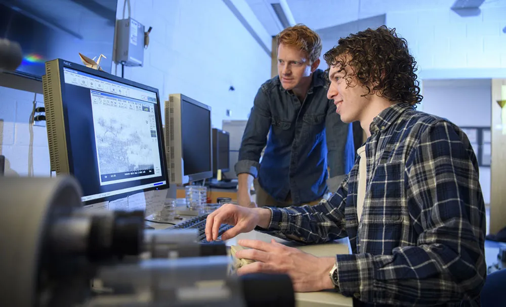
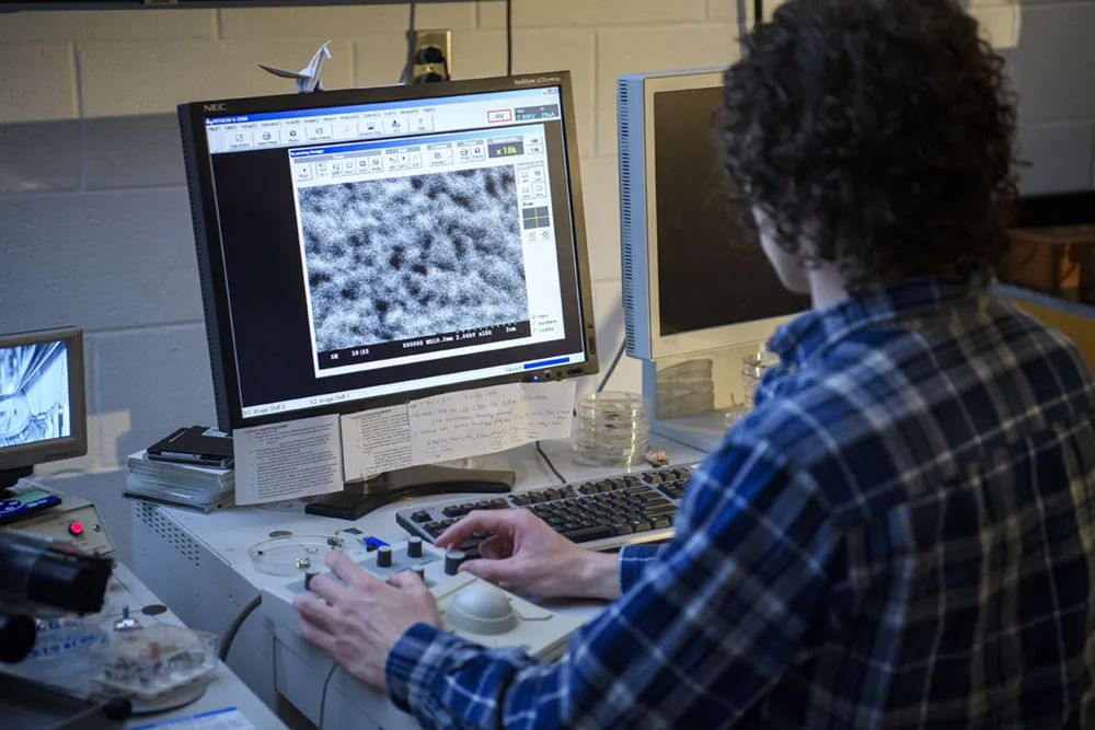
For many researchers, access to advanced instrumentation and toolsets can be the difference between an idea and getting published. But not all academic institutions can prioritize research instrumentation on the same scale.
Jacob Sylvie, an undergraduate researcher at Berry College, experienced this firsthand. His research focused on developing benchtop electrochemical methods to grow crystalline semiconductor materials — work that required highly specialized techniques and tools. Even though Sylvie performed most of his research at Berry, he still had one problem: He needed access to resources that weren’t available on campus.
“Since Berry College is a small, liberal arts, primarily undergraduate institution, we only have access to a limited range of in-house instrumentation,” said Zachary Lindsey, assistant professor at Berry College and Sylvie’s advisor. “The combination of the available instrumentation and focused support offered by expert personnel at Georgia Tech presented a rare, world-class opportunity for my students.”
Sylvie and Lindsey reached out to the Institute for Matter and Systems’ Materials Characterization Facility regarding characterization services. They were advised to apply for the Southeastern Nanotechnology Infrastructure Corridor (SENIC) Catalyst Program to support Sylvie’s research needs.
The program supports researchers in microtechnology, nanotechnology, and the broader scientific community by providing access to SENIC facilities to aid in research, obtain preliminary data, conduct proof-of-concept studies, or for educational purposes.
“One of the goals of SENIC is to democratize access to world-class facilities, like the ones here at IMS,” said David Gottfried, associate director of external user programs and SENIC site director at Georgia Tech. “The Catalyst Seed Grants are one way we can make sure that anyone can benefit from our research infrastructure.”
Through the program, Sylvie and Lindsey received use-of-tool access, staff time, and materials and supplies for six months. During this time, Sylvie published his first peer-reviewed article in Physica B: Condensed Matter. The publication played a pivotal role in his successful application for the Goldwater Scholarship in March.
“I cannot emphasize enough the magnitude of the support and efficiency of the SENIC Catalyst Seed Grant,” said Lindsey. “The impact that this program has had on my students and me is irreplaceable, and I highly recommend that other faculty and students take advantage of this opportunity to push your research to new heights.”
Programs like SENIC don’t just support research — they bridge the gap between potential and achievement, empowering students from all backgrounds to reach new heights in science and innovation.
This work was performed in part at the Georgia Tech Institute for Matter and Systems, a member of the National Nanotechnology Coordinated Infrastructure (NNCI), which is supported by the National Science Foundation (Grant ECCS-2025462).
News Contact
Amelia Neumeister | Research Communications Program Manager
The Institute for Matter and Systems