Aug. 07, 2025
Nazanin Bassiri-Gharb, Harris Saunders, Jr. Chair and Professor in the Woodruff School and MSE, and Yao Xie, Coca-Cola Foundation Chair and Professor in ISyE.

Nazanin Bassiri-Gharb, Harris Saunders, Jr. Chair and Professor in the Woodruff School and MSE, and Yao Xie, Coca-Cola Foundation Chair and Professor in ISyE.

In the world of nanotechnology, seeing clearly isn’t easy. It’s even harder when you’re trying to understand how a material’s properties relate to its structure at the nanoscale. Tools like piezoresponse force microscopy (PFM) help scientists peer into the nanoscale functionality of materials, revealing how they respond to electric fields. But those signals are often buried in noise, especially in instances where the most interesting physics happens.

Now, researchers at Georgia Tech have developed a powerful new method to extract meaningful information from even the noisiest data, or when, alternatively, the response of the material is the smallest. Their approach, which combines physical modeling with advanced statistical reconstruction, could significantly improve the accuracy and confidence of nanoscale measurement properties.

The team’s findings, led by Nazanin Bassiri-Gharb, Harris Saunders, Jr. Chair and Professor in the George W. Woodruff School of Mechanical Engineering and School of Materials Science and Engineering (MSE), are reported in Small Methods.

Co-lead authors Kerisha Williams, a former MSE Ph.D. student, and Henry Shaowu Yuchi, a former Ph.D. student in the H. Milton Stewart School of Industrial and Systems Engineering (ISyE), spearheaded the study. Other collaborators include Kevin Ligonde, a Ph.D. student in the Woodruff School; Mathew Repasky, a former Ph.D. student in ISyE; and Yao Xie, Coca-Cola Foundation Chair and Professor in ISyE.

This research was initiated through Georgia Tech’s Forming Teams and Moving Teams Forward seed grant program, launched by the Office of the Executive Vice President for Research in 2021. Designed to support cross-disciplinary collaboration, the program helps build research teams that align with the growing national emphasis on large-scale, team-based projects. The grant supported early work by Bassiri-Gharb, Xie, and Juan-Pablo Correa-Baena, associate professor and Goizueta Early Career Faculty Chair in MSE.

Read the full story on the George W. Woodruff School of Mechanical Engineering website.

News Contact

Ashley Ritchie
George W. Woodruff School of Mechanical Engineering

Jul. 25, 2025
A white gloved hand holds 3 nuclear pellets with rows of nuclear pellets in the background

Nuclear fuel pellets are primarily made of uranium dioxide (UO2)
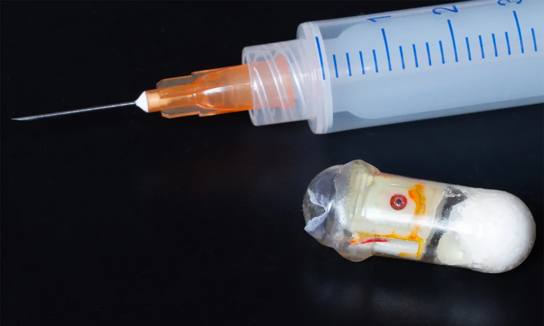
, a ceramic material. They are typically enriched with uranium-235, an isotope that undergoes nuclear fission to produce energy. (Credit: U.S. Nuclear Regulatory Commission)

A woman with dark hair wearing a black blazer smiles

Anna Erickson

A man wearing a dark blue blazer smiles with greenery in the background.

Steven Biegalski

“Nuclear” is a loaded, highly charged word. It can conjure images — both real and imagined — of explosive destruction. 

Nuclear is also a loaded, highly charged technology. A single fuel pellet the size of a pencil eraser contains as much energy as a metric ton of coal, 150 gallons of oil, or 17,000 cubic feet of natural gas. 

The technology’s complex history, along with its vast potential, is why nuclear scientists and engineers often find themselves moonlighting as myth busters. Georgia Tech experts are eager to untangle fact from fiction so nuclear can shine — safely. 

“I am really excited about nuclear, but this is a technology that has a lot of myths and misinformation around it,” said Anna Erickson, Woodruff Professor in the George W. Woodruff School of Mechanical Engineering (ME), and leader of the Consortium for Enabling Technologies and Innovation (ETI), which is focused on nuclear technology. 

“Concerns about nuclear weapons, accidents, and waste have overshadowed nuclear energy’s potential as a clean, carbon-free technology,” she added.

Here, Georgia Tech researchers share what nuclear is, why it’s important, and why its moment is now.

What Is Nuclear? 

“Nuclear, as indicated by its name, is focused on the nucleus within an atom, but also the atom as a whole,” said Steve Biegalski, ME professor and chair of the Nuclear and Radiological Engineering and Medical Physics Program. “From an engineering perspective, we're looking at how we can use the physics of an atom — and the physics of a nucleus — to solve different scientific and societal problems.” 

In 1938, German and Austrian scientists discovered that breaking apart an atom’s nucleus creates energy through fission. Many aspects of nuclear science, however, were advanced through the Manhattan Project during World War II, in which the U.S. developed the atomic bombs it later dropped on Hiroshima and Nagasaki, Japan. This historical association has likely played a significant role in shaping the negative perception of nuclear technology.

But nuclear science isn’t only about international power and weapons, Biegalski said. Advances in nuclear science have contributed to life-saving cancer therapies, cutting-edge heart scans, and on-demand X-ray technologies. 

Safe levels of radiation are all around us — for example, our imported fruits and vegetables are treated with radiation when they enter the country. Even kitty litter is radioactive — not very, but detectable by modern sensors. 

“You might have slightly elevated radioactivity for a short while after you eat a banana in the morning,” Erickson said. “Our bodies have evolved to live with radiation.”

AI Has Entered the Chat

Lately, Erickson has been getting calls from major technology companies with questions about how to power data centers. She isn’t surprised — nuclear energy is widely being discussed as the way to power the AI revolution.

 “Today’s energy needs are very different than they were in the past, and consistent, reliable, and independent electricity production is necessary — especially for the technology sector,” Erickson explained. 

“At this stage, it’s not a question of whether nuclear energy can meet those demands, but how quickly we can make it a reality,” she added. 

One of nuclear’s most distinguishing features is its power density, or how much power is produced by volume of raw material. Another defining feature is its reliability. Wind and solar are weather-dependent and provide power intermittently. Nuclear can supply power around the clock, and data centers require that level of consistency. 

“There are discussions about developing a number of data centers just outside of Atlanta, and those will require full-size nuclear power plants to power them,” Biegalski said. “When we look at electricity production, these facilities need power 24/7, 365 days a year. Nuclear power can supply that, and wind and solar simply cannot.”

Great Power, Great Responsibility

According to Erickson, the nuclear reactors in use today are far more advanced than those associated with past disasters like Chernobyl and Three Mile Island. 

New nuclear plants are designed with great efficiency in mind. Coal must be supplied continuously, whereas nuclear can be loaded once and run for years. 

In addition to dispelling misinformation, nuclear experts are also knowledgeable about nuclear nonproliferation and nuclear security. Georgia Tech is a leader in these areas. Experts like Erickson and Biegalski are regularly tapped to help design new reactors that are popping up across the country.

The Georgia Tech-led nuclear consortium, ETI, assesses how emerging technologies help or hurt nuclear nonproliferation efforts. Nuclear nonproliferation is the global effort to minimize the spread of nuclear weapons, technology, and development. 

“One of our main missions is to understand expansion of civilian nuclear power through the lens of nuclear safeguards and nonproliferation,” Erickson said. “Specifically, we want to know how we can best prevent misuse and mishandling of nuclear materials and keep nuclear facilities safe, while also investing in advancing nuclear technology.”

A Shift in Public Opinion

Despite the popular culture — think Homer Simpson’s nuclear plant job handling green slime — the public is also becoming better informed about nuclear power’s relative safety, especially compared with other energy sources. 

In early 2025, nearly 6 out of 10 Americans supported increased development of nuclear energy. But why are Americans gradually coming around to the idea? 

Erickson may have the answer. “The technology’s potential is catching on across the globe,” she said. “In France, 70% of their electricity comes from nuclear energy.”

For one of her first research projects as a young student, Erickson analyzed what went wrong with the Chernobyl reactors. She understands why people can be wary of nuclear technology.

“Despite the uptick in support for nuclear, people still have concerns we need to answer, rather than just telling people to trust the experts,” Erickson said. “Talking to people is critical in promoting this technology and making sure we keep the public’s trust in this.”

News Contact

Catherine Barzler, Senior Research Writer/Editor
Institute Communications
catherine.barzler@gatech.edu

Jul. 20, 2025
This travel case holds a toolkit containing equipment for inspecting nuclear facilities

This travel case holds a toolkit containing equipment for inspecting nuclear facilities. Dean Calma/IAEA, CC BY

What happens when a country seeks to develop a peaceful nuclear energy program? Every peaceful program starts with a promise not to build a nuclear weapon. Then, the global community verifies that stated intent via the Treaty on the Non-Proliferation of Nuclear Weapons.

Once a country signs the treaty, the world’s nuclear watchdog, the International Atomic Energy Agency, provides continuous and technical proof that the country’s nuclear program is peaceful.

The IAEA ensures that countries operate their programs within the limits of nonproliferation agreements: low enrichment and no reactor misuse. Part of the agreement allows the IAEA to inspect nuclear-related sites, including unannounced surprise visits.

These are not just log reviews. Inspectors know what should and should not be there. When the IAEA is not on site, cameras, tamper-revealing seals on equipment and real-time radiation monitors are working full-time to gather or verify inside information about the program’s activities.

Safeguards Toolkit

The IAEA safeguards toolkit is designed to detect proliferation activities early. Much of the work is fairly technical. The safeguards toolkit combines physical surveillance, material tracking, data analytics and scientific sampling. Inspectors are chemists, physicists and nuclear engineers. They count spent fuel rods in a cooling pond. They check tamper seals on centrifuges. Often, the inspectors walk miles through hallways and corridors carrying heavy equipment.

That’s how the world learned in April 2021 about Iran pushing uranium enrichment from reactor-fuel-grade to near-weapons-grade levels. IAEA inspectors were able to verify that Iran was feeding uranium into a series of centrifuges designed to enrich the uranium from 5%, used for energy programs, to 60%, which is a step toward the 90% level used in nuclear weapons.

Around the facilities, whether for uranium enrichment or plutonium processing, closed-circuit surveillance cameras monitor for undeclared materials or post-work activities. Seals around the facilities provide evidence that uranium gas cylinders have not been tampered with or that centrifuges operate at the declared levels. Beyond seals, online enrichment monitors allow inspectors to look inside of centrifuges for any changes in the declared enrichment process.

Seals verify whether nuclear equipment or materials have been used between onsite inspections.

When the inspectors are on-site, they collect environmental swipes: samples of nuclear materials on surfaces, in dust or in the air. These can reveal if uranium has been enriched to levels beyond those allowed by the agreement. Or if plutonium, which is not used in nuclear power plants, is being produced in a reactor. Swipes are precise. They can identify enrichment levels from a particle smaller than a speck of dust. But they take time, days or weeks. Inspectors analyze the samples at the IAEA’s laboratories using sophisticated equipment called mass spectrometers.

In addition to physical samples, IAEA inspectors look at the logs of material inventories. They look for diversion of uranium or plutonium from normal process lines, just like accountants trace the flow of finances, except that their verification is supported by the ever-watching online monitors and radiation sensors. They also count items of interest and weigh them for additional verification of the logs.

Beyond accounting for materials, IAEA inspectors verify that the facility matches the declared design. For example, if a country is expanding centrifuge halls to increase its enrichment capabilities, that’s a red flag. Changes to the layout of material processing laboratories near nuclear reactors could be a sign that the program is preparing to produce unauthorized plutonium.

Losing Access

Iran announced on June 28, 2025, that it has ended its cooperation with the IAEA. It removed the monitoring devices, including surveillance cameras, from centrifuge halls. This move followed the news by the IAEA that Iran’s enrichment activities are well outside of allowed levels. Iran now operates sophisticated uranium centrifuges, like models IR-6 and IR-9.

Removing IAEA access means that the international community loses insight into how quickly Iran’s program can accumulate weapon-grade uranium, or how much it has produced. Also lost is information about whether the facility is undergoing changes for proliferation purposes. These processes are difficult to detect with external surveillance, like satellites, alone.

a satellite view of a complex of buidlings on a desert landscape
A satellite view of Iran’s Arak Nuclear Complex, which has a reactor capable of producing plutonium. Satellite image (c) 2025 Maxar Technologies via Getty Images

An alternative to the uranium enrichment path for producing nuclear weapons material is plutonium. Plutonium can’t be mined, it has to be produced in a nuclear reactor. Iran built a reactor capable of producing plutonium, the IR-40 Heavy Water Research Reactor at the Arak Nuclear Complex.

Iran modified the Arak reactor under the now-defunct Joint Comprehensive Plan of Action to make plutonium production less likely. During the June 2025 missile attacks, Israel targeted Arak’s facilities with the aim of eliminating the possibility of plutonium production.

With IAEA access suspended, it won’t be possible to see what happens inside the facility. Can the reactor be used for plutonium production? Although a lengthier process than the uranium enrichment path, plutonium provides a parallel path to uranium enrichment for developing nuclear weapons.

Continuity of Knowledge

North Korea expelled IAEA inspectors in 2009. Within a few years, they restarted activities related to uranium enrichment and plutonium production in the Yongbyon reactor. The international community’s information about North Korea’s weapons program now relies solely on external methods: satellite images, radioactive particles like xenon – airborne fingerprints of nuclear activities – and seismic data.

What is lost is the continuity of the knowledge, a chain of verification over time. Once the seals are broken or cameras are removed, that chain is lost, and so is confidence about what is happening at the facilities.

When it comes to IAEA inspections, there is no single tool that paints the whole picture. Surveillance plus sampling plus accounting provide validation and confidence. Losing even one weakens the system in the long term.

The existing safeguards regime is meant to detect violations. The countries that sign the nonproliferation treaty know that they are always watched, and that plays a deterrence role. The inspectors can’t just resume the verification activities after some time if access is lost. Future access won’t necessarily enable inspectors to clarify what happened during the gap.The Conversation


This article is republished from The Conversation under a Creative Commons license. Read the original article.

News Contact

Author:

Anna Erickson, professor of Nuclear and Radiological Engineering, Georgia Institute of Technology


Media Contact:

Shelley Wunder-Smith
shelley.wunder-smith@research.gatech.edu

Jul. 18, 2025
GT logo on an electron microscope

A rare native Atlanta Walter Henderson, Phys 93, associate director for the Materials Characterization Facility and principal research scientist for the Institute for Matter and Systems, jokes that he grew up in “the Stone Age.” But the work that he does managing 12 research leaders who train more than 800 fellow scientists to do over 40,000 hours of work that contributes nearly $400 million in research funding to Georgia Tech each year? That’s positively “Space Age” in nature.

He also notes that they have a surprising amount of fun on the job. For instance, Henderson smiles, consider that time when fast food giant Arby’s asked the team to create the world’s smallest ad by using technology to etch an advertisement onto a sesame seed back in 2018. “We were approached by an ad agency who wanted to earn a Guinness World Record for the smallest sign on the market,” he chuckles. “We used a focused ion beam to do it. It’s a bit like using a laser to inscribe things, except instead of a light beam, it’s this beam of gallium metal ions that you use to etch into samples such as the seed, which also featured the Arby’s logo.”

The ad was then set up at one of their restaurants with an electronic microscope for viewing, given that it was basically about as wide as a human hair, Henderson notes. The agency also made a follow-on internet commercial. “My claim to fame is that I suited up in a bunny suit for them to shoot the video, and some footage in the clean room itself,” he says. “But the actual work was done in our basement-floor Microanalysis lab in the Marcus Nanotechnology Building. In any event, you can still find the ad on YouTube. I just wish I’d had a better agent: I didn’t get any royalties at all, not even, like, a year of free Arby’s.”

It’s not the only time that the facility — a typically serious scientific setting — has been put to equally unique or interesting purposes, though. “For instance, we’ve been asked to analyze pieces of clothing and conduct forensics for crimincal investigations,” notes Henderson. “Given our advanced research equipment, we’ve also been asked to review everything from moon rocks to frogs’ tongues — and practical applications that companies can derive from their scientific properties. On top of it, they’ve also had us test samples and run mechanical property analyses for the Library of Congress and [on] trade secret items for different companies or matters of national security for the government.”

While life inside the lab is fairly routine, Henderson notes, it’s definitely more interesting and varied than some might suspect. “There are certainly moments,” he says. That said, just don’t ask him what happened to the original see, which has since gone AWOL. “I don’t know what happened to it… or if someone at it,” he muses. “But I still have a bottle of sesame seeds in my office, so we could always make a new one.”

by Scott Steinberg, Mgt 99

Read the latest issue of the Georgia Tech Alumni Magazine 

News Contact

Amelia Neumeister | Research Communications Program Manager

Institute for Matter and Systems

Jul. 11, 2025
Computer generated model of nanoparticles

A study from Georgia Tech’s School of Chemical and Biomolecular Engineering introduces LEONARDO, a deep generative AI model that reveals the hidden dynamics of nanoparticle motion in liquid environments. By analyzing over 38,000 experimental trajectories captured through liquid-phase transmission electron microscopy (LPTEM), LEONARDO not only interprets but also generates realistic simulations of nanoscale movement. This innovation marks a major leap in understanding the physical forces at play in nanotechnology, with promising implications for medicine, materials science, and sensor development.

Read the full story.

News Contact

Brad Dixon | Communications Manager

School of Chemical and Biomolecular Engineering

 
Jul. 09, 2025
Photo of Silicon-on-insulator (SOI) wafer

Silicon-on-insulator (SOI) wafer used in a multi-chip module featuring 3D optical interconnects. (Photo: Allison Carter)

A schematic illustration of a multi-chip structure with 3D optical routing.

A schematic illustration of a multi-chip structure with 3D optical routing. The key parts of Adibi's proposed system are: 1) multi-layer planar waveguides, 2) free-form couplers, and 3) a dense vertical waveguide array.

Professor Ali Adibi in front of testing equipment for his 3D optical routing system.

By combining advanced optical techniques, Professor Ali Adibi’s 3D optical routing systems looks to enable vertical chip integration in a way not previously achieved. (Photo: Allison Carter)

The future of computing is lit, literally. 

As microchips grow more complex and data demands intensify, traditional electrical connections are hitting their limits. Speed is king in today’s digital systems, but a major bottleneck remains in how quickly information can move between components like processors and memory. 

This lag is one of the most pressing challenges in advanced hardware design. While processors continue to accelerate, the links that connect them can't keep pace. 

Georgia Tech researcher Ali Adibi is addressing this problem with $5.3 million in funding over three years from the Defense Advanced Research Projects Agency (DARPA). His project is part of DARPA’s Heterogeneous Adaptively Produced Photonic Interfaces (HAPPI) program, which aims to dramatically boost the speed and density of data transmission within microsystems by using light instead of electricity. 

“Optical solutions are highly advantageous for providing the required data rates and power consumptions, and our project is formed to address the most important challenges for achieving the system-level performance,” said Adibi, a professor and Joseph M. Pettit Chair in the School of Electrical and Computer Engineering

The project brings together a multidisciplinary team, including collaborators from the Massachusetts Institute of Technology, University of Florida, NY CREATES, and NHanced Semiconductors, Inc.

Going Vertical 

Unlike traditional optical communication, which connects systems across distances, this project focuses on enabling ultra-fast, low-loss communication withinelectronic systems. 

The key innovation is vertically connecting electronic chips in a compact stack. This design helps overcome the limitations of planar optical routing geometries (layouts that guide light horizontally across a chip) which are often not compatible with the dense, 3D chip architectures needed for next-generation computing. 

Adibi’s team is developing a novel 3D optical routing system that can transmit data with minimal loss, high bandwidth, and compact components. The system is designed to scale to large arrays of interconnected chips with minimal interference between data channels.

Smarter Design with Machine Learning 

At the heart of the project is the use of machine learning (ML) to help design and optimize the light-based communication system.  

ML is used to shape and fine-tune the tiny structures that guide light through and between chips. This includes finding the best sizes, shapes, and layouts for components like couplers and waveguides, so they can be made smaller, work more efficiently, and fit into dense chip layouts.  

“Designing a complete, scalable 3D optical routing structure involves innumerable variables,” Adibi said. “Machine learning helps us navigate that complexity and find solutions that would be nearly impossible to identify manually.” 

Tiny "Mirrors"

Another key innovation involves specialized optical structures, or what Adibi refers to as “artificial mirrors”.

The tiny, precisely shaped structures, called metagratings, are embedded in the chip material to redirect light vertically between layers with minimal loss. These components are designed to guide light efficiently in tight spaces, helping connect stacked chips without losing signal strength. 

“Imagine light traveling through a chip and suddenly being redirected straight up. That’s the kind of precise control we’re achieving,” Adibi explained. 

These innovations, along with advanced techniques for building vertical light paths through thick silicon layers and new packaging solutions that keep components precisely aligned, have shown promise on their own. But combining them is what enables dense, high-speed, low-loss communication between vertically stacked chips, something that no system has achieved before, according to Adibi. 

“As with any complex system, success depends on how well everything is structured and optimized,” he said. “Once everything is in alignment, data can move faster, more efficiently, and with less energy consumption for communicating each bit of data.”


About the Research
This research is supported by the Defense Advanced Research Projects Agency (DARPA) Heterogeneous Adaptively Produced Photonic Interfaces (HAPPI) program. Notice ID DARPA-SN-24-105.

News Contact

Dan Watson

Jul. 01, 2025
An image from Iranian television shows centrifuges lining a hall at Iran’s Natanz uranium enrichment facility in 2021. IRIB via APPEAR

An image from Iranian television shows centrifuges lining a hall at Iran’s Natanz uranium enrichment facility in 2021. IRIB via APPEAR

When U.S. forces attacked Iran’s nuclear facilities on June 21, 2025, the main target was metal tubes in laboratories deep underground. The tubes are centrifuges that produce highly enriched uranium needed to build nuclear weapons.

Inside of a centrifuge, a rotor spins in the range of 50,000 to 100,000 revolutions per minute, 10 times faster than a Corvette engine’s crankshaft. High speeds are needed to separate lighter uranium-235 from heavier uranium-238 for further collection and processing. Producing this level of force means the rotor itself must be well balanced and strong and rely on high-speed magnetic bearings to reduce friction.

Over the years, Iran has produced thousands of centrifuges. They work together to enrich uranium to dangerous levels – close to weapons-grade uranium. Most of them are deployed in three enrichment sites: Natanz, the country’s main enrichment facility, Fordow and Isfahan. Inside of these facilities, the centrifuges are arranged into cascades – series of machines connected to each other. This way, each machine yields slightly more enriched uranium, feeding the gas produced into its neighbor to maximize production efficiency.

As a nuclear engineer who works on nuclear nonproliferation, I track centrifuge technology, including the Iranian enrichment facilities targeted by the U.S. and Israel. A typical cascade deployed in Iran is composed of 164 centrifuges, working in series to produce enriched uranium. The Natanz facility was designed to hold over 50,000 centrifuges.

Iran’s early intentions to field centrifuges on a very large scale were clear. At the peak of the program in the early 2010s it deployed over 19,000 units. Iran later scaled down the number of its centrifuges in part due to international agreements such as the since scrapped Joint Comprehensive Plan of Action signed in 2015.

Legacy of Enrichment

Iran has a long history of enriching uranium.

In the late 1990s, it acquired a Pakistani centrifuge design known as P-1. The blueprints and some components were supplied via the A.Q. Khan black market network – the mastermind of the Pakistani program and a serious source of nuclear proliferation globally. Today, the P-1 design is known as IR-1. IR-1 centrifuges use aluminum and a high-strength alloy, known as maraging steel.

About one-third of the centrifuges that were deployed at the sites of the recent strike on June 21 are IR-1. Each one produces on the order of 0.8 separative work units, which is the unit for measuring the amount of energy and effort needed to separate uranium-235 molecules from the rest of the uranium gas. To put this in perspective, one centrifuge would yield about 0.2 ounces (6 grams) of 60%-enriched uranium-235 per year.

A typical uranium-based weapon requires 55 pounds (25 kilograms) of 90%-enriched uranium. To get to weapons-grade level, a single centrifuge would produce only 0.14 ounces (4 grams) per year. It requires more work to go higher in enrichment. While capable of doing the job, the IR-1 is quite inefficient.

The author explains the uranium enrichment process to CBS News.

More and Better Centrifuges

Small yields mean that over 6,000 centrifuges would need to work together for a year to get enough material for one weapon such as a nuclear warhead. Or the efficiency of the centrifuges would have to be improved. Iran did both.

Before the strike by U.S. forces, Iran was operating close to 7,000 IR-1 centrifuges. In addition, Iran designed, built and operated more efficient centrifuges such as the IR-2m, IR-4 and IR-6 designs. Comparing the IR-1 with the latest designs is like comparing a golf cart with the latest electric vehicles in terms of range and payload.

Iran’s latest centrifuge designs contain carbon fiber composites with exceptional strength and durability and low weight. This is a recipe for producing light and compact centrifuges that are easier to conceal from inspections. According to the international nuclear watchdog International Atomic Energy Agency, before the strike Iran was operating 6,500 IR-2m centrifuges, close to 4,000 IR-4 centrifuges and over 3,000 IR-6 centrifuges.

With each new generation, the separative work unit efficiency increased significantly. IR-6 centrifuges, with their carbon fiber rotors, can achieve up to 10 separative work units per year. That’s about 2.8 ounces (80 grams) of 60%-enriched uranium-235 per year. The International Atomic Energy Agency verified that the IR-6 cascades have been actively used to ramp up production of 60%-enriched uranium.

The most recent and advanced centrifuges developed by Iran, known as IR-9, can achieve 50 separative work units per year. This cuts down the time needed to produce highly enriched uranium for weapon purposes from months to weeks. The other aspect of IR-9 advanced centrifuges is their compactness. They are easier to conceal from inspections or move underground, and they require less energy to operate.

Advanced centrifuges such as the IR-9 drive up the risk of nuclear weapons proliferation significantly. Fortunately, the International Atomic Energy Agency reports that only one exists in testing laboratories, and there is no evidence Iran has deployed them widely. However, it’s possible more are concealed.

Bombs or Talks?

Uranium enrichment of 60% is far beyond the needs of any civilian use. The International Atomic Energy Agency confirmed that Iran stockpiled about 880 pounds (400 kilograms) of highly enriched uranium before the attack, and it might have escaped intact. That’s enough to make 10 weapons. The newer centrifuges – IR-2m, IR-4 and IR-6 – would need a bit over eight months to produce that much.

It’s not clear what the U.S. attack has accomplished, but destroying the facilities targeted in the attack and hindering Iran’s ability to continue enriching uranium might be a way to slow Iran’s move toward producing nuclear weapons. However, based on my work and research on preventing nuclear proliferation, I believe a more reliable means of preventing Iran from achieving its nuclear aims would be for diplomacy and cooperation to prevail.The Conversation


This article is republished from The Conversation under a Creative Commons license. Read the original article.

News Contact

Authors:

Anna Erickson, professor of Nuclear and Radiological Engineering, Georgia Institute of Technology

Media Contact:

Shelley Wunder-Smith
shelley.wunder-smith@research.gatech.edu

Jul. 01, 2025
Tech Tower

Georgia Tech has launched two new Interdisciplinary Research Institutes (IRIs): The Institute for Neuroscience, Neurotechnology, and Society (INNS) and the Space Research Institute (SRI). 

The new institutes focus on expanding breakthroughs in neuroscience and space, two areas where research and federal funding are anticipated to remain strong. Both fields are poised to influence research in everything from healthcare and ethics to exploration and innovation. This expansion of Georgia Tech’s research enterprise represents the Institute’s commitment to research that will shape the future.

“At Georgia Tech, innovation flourishes where disciplines converge. With the launch of the Space Research Institute and the Institute for Neuroscience, Neurotechnology, and Society, we’re uniting experts across fields to take on some of humanity’s most profound questions. Even as we are tightening our belts in anticipation of potential federal R&D budget actions, we also are investing in areas where non-federal funding sources will grow and where big impacts are possible,” said Executive Vice President for Research Tim Lieuwen. "These institutes are about advancing knowledge — and using it to improve lives, inspire future generations, and help shape a better future for us all.”

Both INNS and SRI grew out of faculty-led initiatives shaped by a strategic planning process and campus-wide collaboration. Their evolution into formal institutes underscores the strength and momentum of Georgia Tech’s interdisciplinary research enterprise. 

Georgia Tech’s 11 IRIs support collaboration between researchers and students across the Institute’s seven colleges, the Georgia Tech Research Institute (GTRI), national laboratories, and corporate entities to tackle critical topics of strategic significance for the Institute as well as for local, state, national, and international communities.

"IRIs bring together Georgia Tech researchers making them more competitive and successful in solving research challenges, especially across disciplinary boundaries,” said Julia Kubanek, vice president of interdisciplinary research. “We're making these new investments in neuro- and space-related fields to publicly showcase impactful discoveries and developments led by Georgia Tech faculty, attract new partners and collaborators, and pursue alternative funding strategies at a time of federal funding uncertainty."

The Space Research Institute

The Space Research Institute will connect faculty, students, and staff who share a passion for space exploration and discovery. They will investigate a wide variety of space-related topics, exploring how space influences and intersects with the human experience. The SRI fosters a collaborative community including scientific, engineering, cultural, and commercial research that pursues broadly integrated, innovative projects.


SRI is the hub for all things space-related at Georgia Tech. It connects the Institute’s schools, colleges, research institutes, and labs to lead conversations about space in the state of Georgia and the world. Working in partnership with academics, business partners, philanthropists, students, and governments, Georgia Tech is committed to staying at the forefront of space-related innovation.   


The SRI will build upon the collaborative work of the Space Research Initiative, the first step in formalizing Georgia Tech’s broad interdisciplinary space research community. The Initiative brought together researchers from across campus and was guided by input from Georgia Tech stakeholders and external partners. It was led by an executive committee including Glenn Lightsey, John W. Young Chair Professor in the Daniel Guggenheim School of Aerospace Engineering; Mariel Borowitz, associate professor in the Sam Nunn School of International Affairs; and Jennifer Glass, associate professor in the School of Earth and Atmospheric Sciences. Beginning July 1, W. Jud Ready, a principal research engineer in GTRI’s Electro-Optical Systems Laboratory, will serve as the inaugural executive director of the Space Research Institute.

To receive the latest updates on space research and innovation at Georgia Tech, join the SRI mailing list

The Institute for Neuroscience, Neurotechnology, and Society

The Institute for Neuroscience, Neurotechnology, and Society (INNS) is dedicated to advancing neuroscience and neurotechnology to improve society through discovery, innovation, and engagement. INNS brings together researchers from neuroscience, engineering, computing, ethics, public policy, and the humanities to explore the brain and nervous system while addressing the societal and ethical dimensions of neuro-related research.

INNS builds on a foundation established over a decade ago, which first led to the GT-Neuro Initiative and later evolved into the Neuro Next Initiative. Over the past two years, this effort has culminated in the development of a comprehensive plan for an IRI, guided by an executive committee composed of faculty and staff from across Georgia Tech. The committee included Simon Sponberg, Dunn Family Associate Professor in the School of Physics and the School of Biological Sciences; Christopher Rozell, Julian T. Hightower Chaired Professor in the School of Electrical and Computer Engineering; Jennifer Singh, associate professor in the School of History and Sociology; and Sarah Peterson, Neuro Next Initiative program manager. Their leadership shaped the vision for a research community both scientifically ambitious and socially responsive.

INNS will serve as a dynamic hub for interdisciplinary collaboration across the full spectrum of brain-related research — from biological foundations to behavior and cognition, and from fundamental research to medical innovations that advance human flourishing. Research areas will encompass the foundations of human intelligence and movement, bio-inspired design and neurotechnology development, and the ethical dimensions of a neuro-connected future. 

By integrating technical innovation with human-centered inquiry, INNS is committed to ensuring that advances in neuroscience and neurotechnology are developed and applied ethically and responsibly. Through fostering innovation, cultivating interdisciplinary expertise, and engaging with the public, the institute seeks to shape a future where advancements in neuroscience and neurotechnology serve the greater good. INNS also aims to deepen Georgia Tech’s collaborations with clinical, academic, and industry partners, creating new pathways for translational research and real-world impact.

An internal search for INNS’s inaugural executive director is in the final stages, with an announcement expected soon.

Join our mailing list to receive the latest updates on everything neuro at Georgia Tech.

News Contact

Laurie Haigh
Research Communications

Jul. 08, 2025
Prototype of an "exploding" capsule next to a syringe. The capsule can deliver medications that are typically only effective if injected.

Georgia Tech engineers have created a pill that could effectively deliver insulin and other injectable drugs, making medicines for chronic illnesses easier for patients to take, less invasive, and potentially less expensive.

Along with insulin, it also could be used for semaglutide — the popular GLP-1 medication sold as Ozempic and Wegovy — and a host of other top-selling protein-based medications like antibodies and growth hormone that are part of a $400 billion market.

These drugs usually have to be injected because they can’t overcome the protective barriers of the gastrointestinal tract. Georgia Tech’s new capsule uses a small pressurized “explosion” to shoot medicine past those barriers in the small intestine and into the bloodstream. Unlike other designs, it has no complicated moving parts and requires no battery or stored energy.

This study introduces a new way of drug delivery that is as easy as swallowing a pill and replaces the need for painful injections,” said Mark Prausnitz, who created the pill in his lab with former Ph.D. student Joshua Palacios and other student researchers. 

In animal lab tests, they showed their capsule lowered blood sugar levels just like traditional insulin injections. The researchers reported their pill design and study results DATE in the Journal of Controlled Release.

Read about the technology on the College of Engineering website.

News Contact

Joshua Stewart
College of Engineering

Jun. 24, 2025
 The devices under test will include halide perovskite-based cells, a likely materials platform for next-generation solar cells.

Solar cells account for approximately six percent of the electricity used on Earth; however, in space, they play a significantly larger role, with nearly all satellites relying on advanced solar cells for their power. That’s why Georgia Tech researchers will soon send 18 photovoltaic cells to the International Space Station for a study of how space conditions affect the devices’ operation over time.

“The main goal here is to improve power generation in space,” said Jud Ready, principal research engineer at the Georgia Tech Research Institute (GTRI) and Executive Director of Georgia Tech's Space Research Institute. “The limiting factor on the performance of a spacecraft is usually how much power you can produce. Power, size, weight, complexity, cost – all of these are tied closely to the electrical generation of the solar panels.”

Read the story in the GTRI newsroom.

News Contact

Media Inquiries: gtri.media@gtri.gatech.edu

Writer: John Toon (john.toon@gtri.gatech.edu)
GTRI Communications
Georgia Tech Research Institute
Atlanta, Georgia USA


Subscribe to Matter and Systems