Sep. 27, 2022
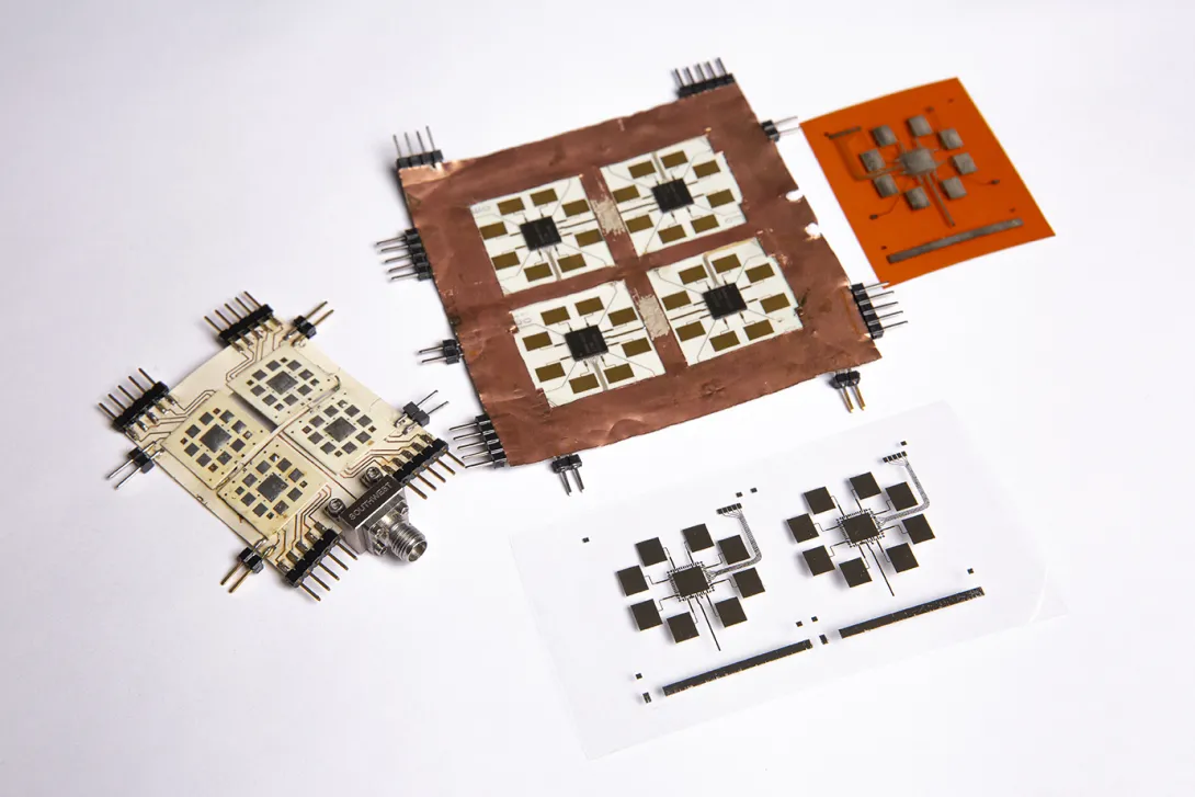
The Scalable Asymmetric Lifecycle Engagement Microelectronics Workforce Development program (SCALE) has announced the program will extend another five years and expand with $10.8 million additional Department of Defense (DoD) funding, with a ceiling of $99 million.
SCALE officials said this expansion of the nation’s preeminent program will further its goal to develop a next-generation workforce that can return the United States to prominence in global microelectronics manufacturing.
Georgia Tech participates in the partnership, which is led by Purdue University and managed by NSWC Crane. SCALE facilitates the training of highly skilled U.S. microelectronics engineers, hardware designers and manufacturing experts. SCALE brings together a public-private-academic partnership of 17 universities and 34 partners within the defense industry and government.
“This is an extremely exciting time in the country and at Tech for microchip design and manufacturing,” said Arijit Raychowdhury, the Steve W. Chaddick School Chair of Tech’s School of Electrical and Computer Engineering (ECE). “These newly announced funds for the SCALE program will help Georgia Tech recruit a new, diverse group of students ready to work in defense microelectronics. We’re thrilled to be a SCALE partner university and honored to be leading many of the project’s specialty areas.”
SCALE provides unique courses, mentoring, internship matching and targeted research projects for college students interested in five microelectronics specialty areas. Georgia Tech ECE faculty members will be the primary investigators for three of the areas:
- system on a chip will be led by Raychowdhury;
- radiation-hardening will be led by John Cressler;
- and heterogeneous integration/advanced packaging will be led by Madhavan Swaminathan.
The other two focus areas are embedded system security/trusted AI and supply chain awareness.
Industry and government partners regularly meet and update a list of knowledge, skills, and abilities important for new entrants to the workforce. The SCALE universities then update their curriculum to ensure the students are prepared for upcoming needs in the rapidly advancing microelectronics field.
Peter Bermel, SCALE director and the Elmore Associate Professor of Electrical and Computer Engineering at Purdue, said the United States will need 50,000 trained semiconductor engineers to meet overwhelming and rapidly growing demand.
“The United States is committed to expanding and strengthening its semiconductor industry and workforce rapidly over the next five years,” Bermel said. “SCALE takes a holistic approach to the microelectronics workforce gap by comprehensively addressing system challenges for workforce training and recruiting.”
Goals for the next five years include:
- Expanding student participation in SCALE fivefold to more than 1,000.
- Developing learning models for K-12 classrooms.
- Collaborating with community colleges nationwide to develop microelectronics classes.
The demand for microelectronics increased by 26.2% in 2021. But while the United States consumes about half of the chips produced worldwide, the country only manufactures about 12%, highlighting the pressing need for the U.S. to strengthen its domestic semiconductor supply chains and increase industrial capacity.
The funding announcement is the latest highlight in Georgia Tech’s leadership role in bolstering microelectronics and workforce development. Tech’s large engineering and science faculty bring a broad set of research expertise to strengthen the country’s semiconductor capacity. The Institute is uniquely positioned to train the microelectronics workforce, drive future microelectronics advances, and provide fabrication and packaging facilities for industry, academic and government partners to develop and test new solutions.
###
The Georgia Institute of Technology, or Georgia Tech, is a top 10 public research university developing leaders who advance technology and improve the human condition. The Institute offers business, computing, design, engineering, liberal arts, and sciences degrees. Its nearly 44,000 students, representing 50 states and 149 countries, study at the main campus in Atlanta, at campuses in France and China, and through distance and online learning. As a leading technological university, Georgia Tech is an engine of economic development for Georgia, the Southeast, and the nation, conducting more than $1 billion in research annually for government, industry, and society.
News Contact
Dan Watson
dwatson@ece.gatech.edu
Aug. 05, 2022
The Materials Characterization Facility (MCF) at Georgia Tech has installed a new inorganic m spectrometry facility. The facility includes two new inductively couple plasma mass spectrometry (ICP-MS) systems: a Thermo iCAP RQ quadrupole ICP-MS for streamlined and high-throughput determinations of elemental concentrations and a Thermo Neoma multicollector ICP-MS with collision cell technology for the precise determinations of isotope ratios within a given sample.
Each instrument can measure elemental variability in both dissolved aqueous samples as well as solids/minerals via laser ablation microsampling from a Teledyne Iridia laser ablation system. Together the system can measure isotopes at precision in elemental systems from Li and U.
Planned applications include: (1) high-resolution measurements of Ca, Sr, Ba, Mg, and B elemental and isotopic variability in seawater and marine and terrestrial carbonates for paleoclimate reconstructions, (2) (U-Th)/Pb dating and Hf isotope measurements to study the origin of critical mineral deposits, with a potential engineering application and the development of novel methods for increasing precision/accuracy and minimizing sample consumption during routine analyses of water quality and environmental contamination.
The MCF welcomes users interested in these and other potential applications of this new facility to their scientific and engineering research to contact David Tavakoli (atavakoli6@gatech.edu).
News Contact
David Tavakoli (atavakoli6@gatech.edu).
Jul. 18, 2022

The American Society of Mechanical Engineers (ASME) has honored Georgia Tech aerospace engineering professor George Kardomateas with the Spirit of St. Louis Medal for exemplary work in the progress of aeronautics and astronautics. He is in great company as Daniel Guggenheim, Neil A. Armstrong, John E. Northrup, John W. Young (AE 1952), George W. Lewis, Charles S. Draper, Robert G. Lowey, Michael Collins, and the late Dewey Hodges have also received this premier medal. ASME will present Kardomateas with the medal at the International Mechanical Engineering Congress & Exposition in Columbus, Ohio, October 30-November 3, 2022.
Kardomateas has spent over thirty years improving aircrafts from a structural standpoint. More specifically he investigates ways to ensure that aerospace structures retain their structural integrity. He focuses on the special part of mechanics called fracture mechanics, which studies the conditions for the initiation and propagation of cracks and debonds. “Fracture mechanics and damage tolerance have been very successful in that, nowadays, airplanes don’t usually come down because of structural failure,” explained Kardomateas.
He credits his lifelong scientific triumphs to his education in the United States and Greece, his collaboration with past and present colleagues at Georgia Tech, and the academic system in America. “The environment at Georgia Tech fosters collaboration and innovation. The higher education system provides opportunities through the collegial network in scientific forums where ideas can be exchanged with those inside and outside of your institution.” Former AE School professors, including the late Bob Carlson, and George Simitses, inspired him as colleagues and also acted as mentors to him.
Kardomateas earned a diploma from the National Technical University of Athens in Greece and both his master’s and doctoral degrees from the Massachusetts Institute of Technology. In 1989, he joined the School of Aerospace Engineering's faculty at the Georgia Tech. He has authored three books, An Introduction to Fatigue in Metals and Composites, Structural and Failure Mechanics of Sandwich Composites, and Mechanics of Failure Mechanisms in Structures. He is also the editor of six volumes on the topic of failure mechanics of composite and sandwich structures, an associate editor of the Handbook of Damage Mechanics: Nano to Macro Scale for Materials and Structures, as well as the author of about 200 papers published in refereed journals or as parts of books.
In addition to his work at Georgia Tech, he has served the discipline in several capacities. The ASME Fellow has operated as an Associate Editor of the Journal of Applied Mechanics, and the AIAA Journal, as a Contributing Editor of the International Journal of Non-Linear Mechanics and as a guest editor of the International Journal of Solids and Structures and the Journal of Mechanics of Materials and Structures. In addition, he has served as the technical chair of the 2014 ASME Congress, general chair of the 2015 ASME Congress, and the steering committee chair of the 2017 ASME Congress. He was the elected chairman of the Applied Mechanics Division Composites Committee and the program representative of the Aerospace Division Structures and Materials Committee. Kardomateas has also served in many other panels and committees including as the Chair of the Daniel Guggenheim Medal Award Board, and on the Organizing Committee of the sixth, seventh, tenth and eleventh Institute for Advanced Composites Manufacturing’s International Conferences on Sandwich Structures; he has also served on external evaluation committees for many academic programs.
Currently, the medal winner is working on his next book that focuses on the fracture and fatigue of metallic and composite aerospace structures, which will include his latest research advances in the field.
News Contact
Monique Waddell
Mar. 29, 2022
5G+ (5G/Beyond 5G) is the fastest-growing segment and the only significant opportunity for investment growth in the wireless network infrastructure market, according to the latest forecast by Gartner, Inc. But currently 5G+ technologies rely on large antenna arrays that are typically bulky and come only in very limited sizes, making them difficult to transport and expensive to customize.
Researchers from Georgia Tech’s College of Engineering have developed a novel and flexible solution to address the problem. Their additively manufactured tile-based approach can construct on-demand, massively scalable arrays of 5G+ (5G/Beyond 5G)‐enabled smart skins with the potential to enable intelligence on nearly any surface or object. The study, recently published in Scientific Reports, describes the approach, which is not only much easier to scale and customize than current practices, but features no performance degradation whenever flexed or scaled to a very large number of tiles.
“Typically, there are a lot of smaller wireless network systems working together, but they are not scalable. With the current techniques, you can’t increase, decrease, or direct bandwidth, especially for very large areas,” said Manos Tentzeris, Ken Byers Professor in Flexible Electronics in the School of Electrical and Computer Engineering. “Being able to utilize and scale this novel tile-based approach makes this possible.”
Tentzeris says his team’s modular application equipped with 5G+ capability has the potential for immediate, large-scale impact as the telecommunications industry continues to rapidly transition to standards for faster, higher capacity, and lower latency communications.
BUILDING THE TILES
In Georgia Tech’s new approach, flexible and additively manufactured tiles are assembled onto a single, flexible underlying layer. This allows tile arrays to be attached to a multitude of surfaces. The architecture also allows for very large 5G+ phased/electronically steerable antenna array networks to be installed on-the-fly. According to Tentzeris, attaching a tile array to an unmanned aerial vehicle (UAV) is even a possibility to surge broadband capacity in low coverage areas.
In the study, the team fabricated a proof-of-concept, flexible 5×5-centimeter tile array and wrapped it around a 3.5-centimeter radius curvature. Each tile includes an antenna subarray and an integrated, beamforming integrated circuit on an underlying tiling layer to create a smart skin that can seamlessly interconnect the tiles into very large antenna arrays and massive multiple-input multiple-outputs (MIMOs) — the practice of housing two or more antennas within a single wireless device. Tile-based array architectures on rigid surfaces with single antenna elements have been researched before, but do not include the modularity, additive manufacturability, or flexible implementation of the Georgia Tech design.
The proposed modular tile approach means tiles of identical sizes can be manufactured in large quantities and are easily replaceable, reducing the cost of customization and repairs. Essentially, this approach combines removable elements, modularity, massive scalability, low cost, and flexibility into one system.
5G+ IS JUST THE BEGINNING
While the tiling architecture has demonstrated the ability to greatly enhance 5G+ technologies, its combination of flexible and conformal capabilities has the potential to be applied in numerous different environments, the Georgia Tech team says.
“The shape and features of each tile scale can be singular and can accommodate different frequency bands and power levels,” said Tentzeris. “One could have communications capabilities, another sensing capabilities, and another could be an energy harvester tile for solar, thermal, or ambient RF energy. The application of the tile framework is not limited to communications.”
Internet of Things, virtual reality, as well as smart manufacturing/Industry 4.0 — a technology-driven approach that utilizes internet-connected “intelligent” machinery to monitor and fully automate the production process — are additional areas of application the team is excited to explore.
“The tile-architecture’s mass scalability makes its applications particularly diverse and virtually ubiquitous. From structures the size of dams and buildings, to machinery or cars, down to individual health-monitoring wearables,” said Tentzeris. “We’re moving in a direction where everything will be covered in some type of a wireless conformal smart skin encompassing electronically steerable antenna arrays of widely diverse sizes that will allow for effective monitoring.”
The team now looks forward to testing the approach outside the lab on large, real-world structures. They are currently working on the fabrication of much larger, fully inkjet-printed tile arrays (256+ elements) that will be presented at the upcoming International Microwave Symposium (IEEE IMS 2022) – the flagship IEEE conference in RF and microwave engineering. The IMS presentation will introduce a new tile-based large-area architecture version that will allow assembly of customizable tile arrays in a rapid and low-cost fashion for numerous conformal platforms and 5G+ enabled applications.
****
The authors declare no competing interests.
This work was supported in part by the National Science Foundation.
CITATIONS: He, X., Cui, Y. & Tentzeris, M.M. Tile-based massively scalable MIMO and phased arrays for 5G/B5G-enabled smart skins and reconfigurable intelligent surfaces. Sci Rep 12, 2741 (2022). https://doi.org/10.1038/s41598-022-06096-9
K.Hu, G.S.V.Angulo, Y.Cui and M.M.Tentzeris, “Flexible and Scalable Additively Manufactured Tile-Based Phased Arrays for Satellite Communications and 5G mmWave Applications,” accepted for presentation at IEEE International Microwave Symposium (IMS) 2022, Denver, CO, June 2022.
News Contact
Dan Watson
dwatson@ece.gatech.edu
Jan. 21, 2022
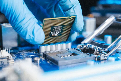
This country’s semiconductor chip shortage is likely to continue well into 2022, and a Georgia Tech expert predicts that the U.S. will need to make major changes to the manufacturing and supply chain of these all-important chips in the coming year to stave off further effects.
That includes making more of these chips here at home.
Madhavan Swaminathan is the John Pippin Chair in Electromagnetics in the School of Electrical and Computer Engineering. He also serves as director of the 3D Systems Packaging Research Center.
As an author of more than 450 technical publications who holds 29 patents, Swaminathan is one of the world’s leading experts on semiconductors and the semiconductor chips necessary for many of the devices we use every day to function.
“Almost any consumer device that is electronic tends to have at least one semiconductor chip in it,” Swaminathan explains. “The more complicated the functions any device performs, the more chips it is likely to have.”
Some of these semiconductor chips process information, some store data, and others provide sensing or communication functions.
In short, they are crucial in devices from video games and smart thermostats to cars and computers.
Our current shortage of these chips began with the Covid-19 pandemic. When consumers started staying at home and car purchases took a downward turn, chip manufacturers tried to shift to make more chips for other goods like smartphones and computers.
But Swaminathan explains that making that kind of switch is not simple. Entire production operations have to be changed. The chips are highly sensitive and can be damaged by static electricity, temperature variations, and even tiny specks of dust. The manufacturing environments must be highly regulated, and changes in the process can add months.
The pandemic highlighted another challenge with the semiconductor chip industry, according to Swaminathan.
“There’s a major shortage of companies making chips,” he says. “If you look worldwide, there are maybe four or five manufacturers making 80-90% of these chips and they are located outside of the United States.”
This creates supply chain hiccups with the raw supplies needed to make these chips as well. Add in the fact that many of these companies only design their chips – they don’t manufacture them directly.
“American consumers use 50% of the world’s chips,” Swaminathan says, which creates a serious challenge when the overwhelming majority of those chips are manufactured in other nations.
In the short term, the costs of the chip shortage is being passed on to the consumer. We see this directly with products like PlayStations and Xboxes that are more and more expensive and harder to purchase when the chips necessary for the consoles to function are in short supply.
Beyond 2022, Swaminathan says we need to work to revitalize the industry domestically.
“We need to bring more manufacturing back to the United States,” he says. “The U.S. government has recognized the importance of this semiconductor chip shortage and is trying to address the issue directly.”
That means investing in new plants to manufacture the chips, but America's journey toward chip self-sufficiency will continue to be a work in progress.
“This is a cycle,” Swaminathan explains. “But this is probably the first time where it has had such a major effect in so many different industries.”
But consumers can take direct action on their own in the coming year. “Reduce the number of times you purchase or upgrade electronic devices like phones and cars,” he says. “Then it becomes just a supply problem, not a demand and supply problem.”
Dec. 14, 2021
The Georgia Institute of Technology was awarded a grant from the U.S. Department of Commerce’s Economic Development Administration (EDA) as part of its $1 billion Build Back Better Regional Challenge. Georgia Tech is one of 60 entities to be awarded funding to assist communities nationwide in their efforts to accelerate the rebuilding of their economies in the wake of the pandemic.
As a leader in artificial intelligence, manufacturing research, and innovation-led economic development, Georgia Tech will utilize the grant for technical assistance to plan the Georgia Artificial Intelligence Manufacturing Corridor (GA-AIM). Led by Thomas Kurfess and Aaron Stebner in the George W. Woodruff School of Mechanical Engineering and in collaboration with local partners, GA-AIM will fill existing technology gaps, build a technological opportunity framework that includes underrepresented communities and rural Georgia counties, and better secure the state’s manufacturing infrastructure.
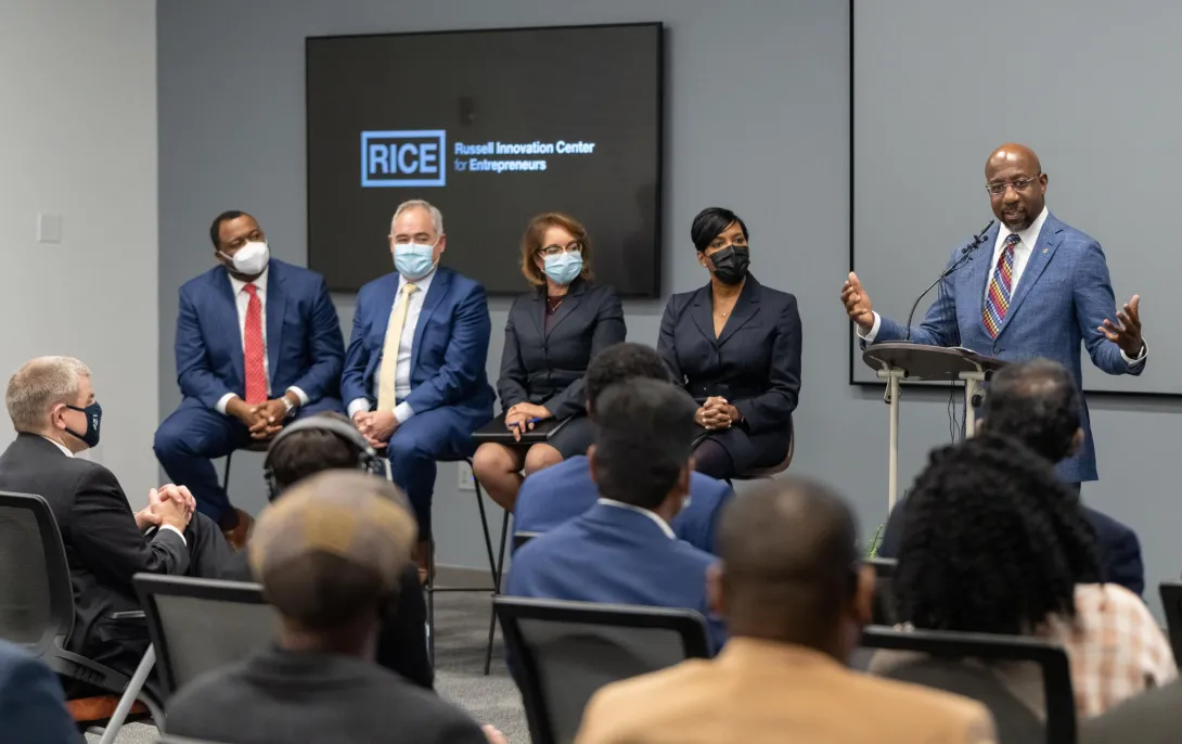
Georgia Tech’s partners in the effort include the Russell Innovation Center for Entrepreneurs, Spelman College, the Technical College System of Georgia, and the Georgia Department of Economic Development.
“We are truly honored to be awarded this grant to implement our vision for manufacturing excellence in Georgia with our partners in artificial intelligence research,” said Chaouki T. Abdallah, executive vice president for Research at Georgia Tech. “Alongside these important partners, the grant enables us to collaborate to include diverse backgrounds and perspectives in the process of learning, discovery, and creation, furthering Georgia Tech’s mission to expand access.”
Georgia Tech and its partners will pair artificial intelligence and manufacturing research innovation to better secure the manufacturing ecosystem, expand opportunity to distressed and rural communities and underrepresented groups, and support business growth across the state.
“We are thrilled to help communities work together — in coalitions of government, nonprofits, academia, the private sector, and others — to craft ambitious and regionally unique plans to rebuild their communities,” said Alejandra Y. Castillo, assistant secretary of commerce for the EDA. “These projects will help revitalize local economies and tackle our biggest challenges related to climate change, manufacturing, supply chains, and more. EDA is proud to ignite these plans and help communities nationwide build back better.”
GA-AIM’s partners have created a complementary network of resources that focus on each partner organization’s expertise and mission.
“We have an opportunity to create meaningful impact at the intersection of AI and manufacturing,” said Stebner, who wrote the grant proposal that resulted in the $500,000 grant from EDA.
Kurfess, who serves as the regional economic competitiveness officer for the grant, added, “Bringing together AI and manufacturing will ensure a strong manufacturing base for Georgia that will leverage our well-trained workforce and our strong educational institutions that are participating in this effort. What excites me the most is that AI will augment our workforce, making it more valuable and productive, ensuring job growth for Georgia and the U.S. well into the future.”
The GA-AIM effort takes a multifaceted approach to address its core goals:
Georgia Tech
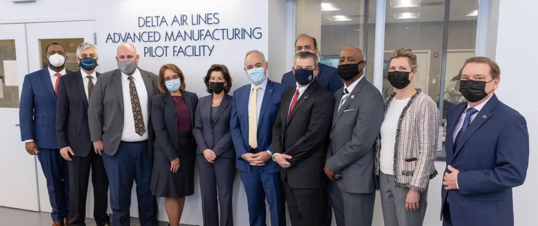
- Formation of the AI Manufacturing Pilot Facility: Georgia Tech’s Advanced Manufacturing Pilot Facility will be transformed into the AI Manufacturing Pilot Facility. The new facility allows for government pilot trials, cybersecurity games, and workforce training to innovate, transition, and create a workforce for AI manufacturing technologies without exposing the region’s supply chains to risk.
- Center for AI Commercialization: Two of Georgia Tech’s commercialization programs — VentureLab and I-Corps South — will create a center for the commercialization of AI manufacturing technologies into local and regional startups. Those commercialization efforts will occur through a quarterly cohort-based entrepreneurial training program built on the National Science Foundation’s I-Corps curriculum. The center will also provide training for instructors to build a sustainable workforce and will secure investment funding for these startups.
- AI Manufacturing Community Engagement: The Enterprise Innovation Institute, Georgia Tech’s chief economic development arm, will engage in focused outreach and technical assistance to small and mid-sized manufacturers and minority business enterprises through its Georgia Manufacturing Extension Partnership and Georgia Minority Business Development Agency Business Center programs. A third Enterprise Innovation Institute program, the Economic Development Lab, will focus on outreach and engagement in distressed and underserved parts of the state, create workforce development programs and implementation strategies, and attract outside investment.
- AI Manufacturing Rural Supply Chain: The Supply Chain and Logistics Institute will study the impact of automation technologies, build automation solutions tailored for rural manufacturers, and create programs that lower the barrier for rural manufacturers’ access to use the AI Manufacturing Pilot Facility.
- AI InVenture K-12 Experiences: To ensure a technically capable workforce in the coming years, Georgia Tech’s InVenture Prize and the Center for Education Integrating Science, Mathematics, and Computing will expand their emphasis to rural and underserved areas of the state by piloting a rural regional event with a region-specific prize. They will also create supplemental lessons centered on AI and data science that will be part of a K-12 InVenture Prize curriculum website.
Spelman College
- Virtual Reality for AI Workforce Training Innovation: Spelman’s Innovation Lab will develop virtual reality technology for training or retraining the GA-AIM workforce to make workers comfortable with new technologies before deployment in real-world applications.
Russell Innovation Center for Entrepreneurs
- LaunchPad AI Innovation Studio: The Russell Innovation Center for Entrepreneurs will create the 5,000-square-foot LaunchPad AI Innovation Studio to provide prototyping and proof of concept development of physical products. Black entrepreneurs will be given access to equipment, training, and mentoring. LaunchPad AI will also be open to AI InVenture teams from Atlanta’s K-12 public schools, with special programs designed for startup mentoring and seed funding for K-12 entrepreneurs.
Technical College System of Georgia (TCSG)
- AI Manufacturing Technical Workforce Development: As Georgia’s technical college coordinating organization, the TCSG will design, develop, and implement curricula at community colleges that include apprenticeships at AI-MPF and virtual reality modules from Spelman. The TCSG will also provide regional entry points for dual enrollment and traditional students to AI manufacturing technical education at certificate and degree levels. Graduates will have exit points that lead directly to careers in the industry or provide for the continuation of education and higher degree attainment through articulation agreements among GA-AIM members.
With this grant, Tech becomes a finalist for significantly more funding to implement projects that support an industry sector and help communities withstand future economic shocks.
“GA-AIM is in strategic alignment with the EDA’s funding priorities, including manufacturing, workforce development, equity, and technology-based economic development,” said David Bridges, vice president of the Enterprise Innovation Institute at Georgia Tech and co-author of the grant proposal. “With manufacturing employing more than 400,000 people across the state and contributing more than $61 billion in economic activity, it’s critical that we leverage the best ideas and programs through our coalition of partners.”
###
About the Georgia Institute of Technology
The Georgia Institute of Technology, or Georgia Tech, is a top 10 public research university developing leaders who advance technology and improve the human condition. The Institute offers business, computing, design, engineering, liberal arts, and sciences degrees. Its nearly 44,000 students, representing 50 states and 149 countries, study at the main campus in Atlanta, at campuses in France and China, and through distance and online learning. As a leading technological university, Georgia Tech is an engine of economic development for Georgia, the Southeast, and the nation, conducting more than $1 billion in research annually for government, industry, and society.
About the U.S. Economic Development Administration
The mission of the U.S. Economic Development Administration (EDA) is to lead the federal economic development agenda by promoting competitiveness and preparing the nation's regions for growth and success in the worldwide economy. An agency within the U.S. Department of Commerce, EDA makes investments in economically distressed communities in order to create jobs for U.S. workers, promote American innovation, and accelerate long-term sustainable economic growth.
Writer: Péralte C. Paul I peralte.paul@comm.gatech.edu I 404.316.1210
Media contact: Steven Norris | stephen.norris@comm.gatech.edu| 404.281.3343
News Contact
Péralte C. Paul
404.316.1210
Dec. 03, 2021

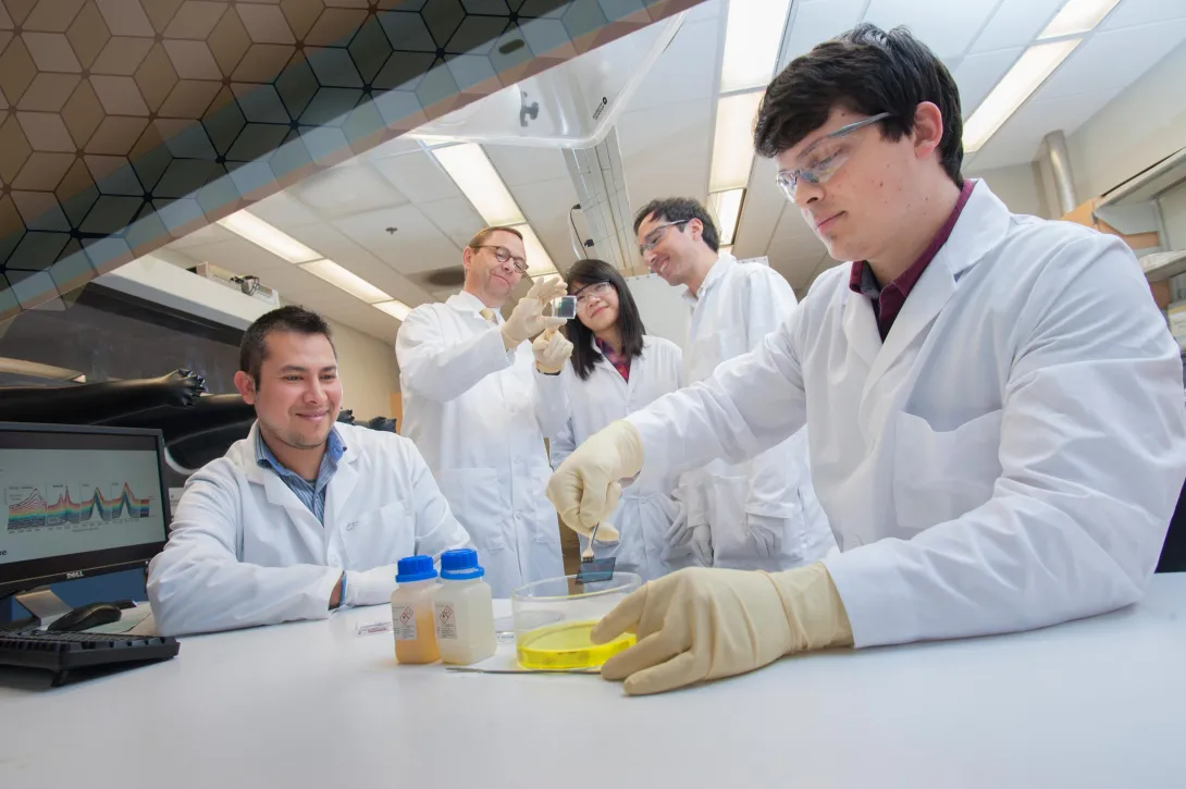
With holiday shopping deadlines looming, consumers cannot escape the impact of the global microelectronic chip shortage. From daily news reports about manufacturers unable to complete orders due to the lack of chips, to “out of stock” messages across websites on popular electronics items, one of the impacts of COVID was to lay bare the massive importance of the microelectronic chip in daily modern life, and how a single-location centered manufacturing nexus can upend the consumer market on a massive scale. The combination of these real-world impacts on supply chains, as well as the need to localize semiconductor and chip manufacturing gave Congress the impetus to pass the “Creating Helpful Incentives to Produce Semiconductors for America Act (CHIPS)”. CHIPS seeks to increase investments and incentives to support U.S. semiconductor manufacturing, research and development, and supply chain security.
The Georgia Institute of Technology was the first university to offer a comprehensive curriculum on microelectronics and microsystems design and packaging and, currently, numerous faculty at Georgia Tech are widely known for their work in semiconductor and microelectronics technologies. In December of 2021 Georgia Tech researchers will again showcase how their pushes the boundaries of microelectronics technologies at the IEEE International Electron Devices Meeting (IEDM).
The School of Electrical and Computer Engineering research teams of Assistant Professor Asif Khan, partnering with Dan Fielder Professor Muhannad Bakir, and Associate Professor Shimeng Yu, partnering with Professor Sung-Kyu Lim and Assistant Professor Shaolan Li, have dominated the 2021 IEDM presentation line-up with a total of 8 accepted papers. With topics ranging from ferroelectric materials for memory, new advances in ALD process, and in-memory computing and 3D reconfigurable architectures, the research presented by these teams is at the cutting-edge of advancing computing power and consumer electronics. In addition to the research presentations, Electrical and Computing Engineering Faculty & Director of the 3D Systems Packaging Research Center at GT will be presenting a short course session on devoted to “Heterogenous Integration Using Chiplets & Advanced Packaging”
Noting the timely nature of these research advancements, Arijit Raychowdhory; Professor and Steve W. Chaddick School Chair in Electrical and Computer Engineering noted, “IEDM is a premier conference in the area of semiconductor devices. Such a strong performance by GT ECE exemplifies the strength of our program, the ingenuity of our students and the innovation driven by our world-class faculty. Sincere congratulations to Professors Khan, Yu Bakir, Lim and Li for their pioneering research in semiconductor logic and memory technologies, that are critical for our nation and our industries.”
Asif Khan is an assistant professor in the School of Electrical and Computer Engineering at the Georgia Tech. He received his Ph.D. in electrical engineering and computer sciences from the University of California, Berkeley in 2015. His work led to the first experimental proof-of-concept demonstration of the negative capacitance effect in ferroelectric oxides. His group at Georgia Tech conceptualizes and fabricates electronic devices that leverage interesting physics and novel phenomena in emerging materials (such as ferroelectrics, antiferroelectrics and strongly correlated systems) to overcome the “fundamental” limits in computation and to address the most pressing challenges in electronics and the semiconductor industry.
Shimeng Yu is currently an associate professor in the School of Electrical and Computer Engineering at the Georgia Tech. He received the B.S. degree in microelectronics from Peking University in 2009, and the M.S. degree and Ph.D. degree in electrical engineering from Stanford University in 2011 and 2013, respectively. From 2013 to 2018, he was an assistant professor at Arizona State University. Prof. Yu’s research interests are the semiconductor devices and integrated circuits for energy-efficient computing systems. His research expertise is on the emerging non-volatile memories for applications such as deep learning accelerator, in-memory computing, 3D integration, and hardware security.
Muhannad S. Bakir is the Dan Fielder Professor in the School of Electrical and Computer Engineering at Georgia Tech. Dr. Bakir and his research group have received more than thirty paper and presentation awards including six from the IEEE Electronic Components and Technology Conference (ECTC), four from the IEEE International Interconnect Technology Conference (IITC), one from the IEEE Custom Integrated Circuits Conference (CICC), and two from the IEEE Transactions on Components Packaging and Manufacturing Technology (TCPMT). Muhannad S. Bakir received the B.E.E. degree from Auburn University, Auburn, AL, in 1999 and the M.S. and Ph.D. degrees in electrical and computer engineering from the Georgia Tech in 2000 and 2003, respectively. His research interests include, heterogeneous microsystem design and integration, including 2.5D and 3D ICs and packaging, electrical and photonic interconnects, and embedded cooling technologies.
Sung Kyu Lim received B.S. (1994), M.S. (1997), and Ph.D. (2000) degrees all from the Computer Science Department at UCLA. During 2000-2001, he was a post-doctoral scholar at UCLA, and a senior engineer at Aplus Design Technologies, Inc. Lim joined the School of Electrical and Computer Engineering at Georgia Institute of Technology an assistant professor. He is currently the director of the GTCAD (Georgia Tech Computer Aided Design) Laboratory and focuses on VLSI and 3D circuit architecture and packaging.
Shaolan Li received his B.Eng. degree with highest honor from the Hong Kong University of Science and Technology (HKUST) in 2012, and his Ph.D. from UT Austin in 2018, all in electrical engineering. Prior joining Georgia Tech as an assistant professor in 2019, he was a post-doctoral fellow in the Department of Electrical and Computer Engineering at UT Austin from 2018-2019. He also held intern positions in Broadcom Ltd. in Sunnyvale, California, and NXP in Tempe, Arizona during 2013-2014. His research interests are broadly in analog, mixed-signal, and RF integrated circuits. His expertise is in high-performance data converters, ultra-low-power low-cost sensor interface, and novel analog mixed-signal architectures for design automation.
The IEEE International Electron Devices Meeting (IEDM) is the world’s preeminent forum for reporting technological breakthroughs in the areas of semiconductor and electronic device technology, design, manufacturing, physics, and modeling. IEDM is the flagship conference for nanometer-scale CMOS transistor technology, advanced memory, displays, sensors, MEMS devices, novel quantum and nano-scale devices and phenomenology, optoelectronics, devices for power and energy harvesting, high-speed devices, as well as process technology and device modeling and simulation. Georgia Tech research teams have a strong track of record in IEDM publications in the recent years, including 8, 4, 9 and 7 papers presented in IEDM 2018, 2019, 2020 and 2021, respectively.
- Christa M. Ernst
News Contact
Christa M. Ernst - Interdisciplinary Research Communications Program Manager
Topics: Materials | Nanotechnology | Robotics
Georgia Institute of Technology| christa.ernst@research.gatech.edu
Oct. 19, 2021
1. What is your field of expertise and at what point in your life did you first become interested in this area?
I work at the intersection of mechanics, metallurgy, machine learning, and manufacturing. I became interested in engineering as a small child – my grandfather was an engineer, and when I would spend time with my grandparents in the summer, I would go to work with him, and I was fascinated with drawing boards, alligator clips, circuits, and more. In high school, I started interning at the business he had built that primarily developed automation and test equipment for circuit breaker manufacturing (he had passed and my uncle then ran it). I started in the stock room, worked through the machine shop, assembly, and into quality control in my first years there. Then I became an engineering assistant as I went into my undergraduate studies. I had thought that I wanted to be electrical engineer (like my grandfather), but after 6 – 8 months of assisting EE, I realized that my true passion was in mechanical engineering, and I moved over to ME – so that foundation instilled in me that I had a passion for ME, manufacturing, and automation. The metallurgy came years later, when I won a graduate fellowship to work at NASA Glenn while earning my Master’s degree. I worked with metallurgists there who were developing new shape memory alloys, which fascinated me. I resisted materials science and metallurgy for many years, insisting that should be someone else’s job, and I should stick to manufacturing and ME. However, it became evident that you can’t engineer with shape memory alloys or develop their manufacturing unless you deeply understood their metallurgy – that resonated with me when I attended a conference in 2008 while working for a startup company that was commercializing some of the new shape memory alloys the group I’d worked with at NASA had developed. When I returned from that conference, I signed up for my PhD program the next week and dove deep into the intersection of metallurgy, manufacturing, and mechanics. The machine learning came years later, several years into my faculty career. We were working with several companies and the state Office of Economic Development in Colorado (I started my faculty career at Colorado School of Mines) to develop an R&D center and technology incubator to support the growing metals 3D printing industry. When I asked the industry people why they needed a center/consortium at Mines in this area – what were they not getting at other additive manufacturing centers at that time (this was 2014/2015), they said “no one is helping us with our data problems.” So, that became our mission – data informatics innovations in metals additive manufacturing. Here at GT, I’m thrilled by the opportunities, colleagues, and infrastructure available to bring it all together – our big vision for this IMat initiative is to develop R&D test beds and technology incubators for AI materials manufacturing.
2. Why is your theme area important to the development of Georgia Tech’s Materials research strategy?
Largely, our materials research laboratories (nation-wide and globally, not just at Georgia Tech) have been designed and built to support human operators. However, AI cannot independently function in the same way and in the same environments – or, at least, we will never realize its full potential if we make it play by our rules. Re-thinking and designing new materials laboratories that can operate autonomously and semi-autonomously is critical to be at the forefront of future innovations.
3. What are the broader global and social benefits of the research you and your team conduct?
Lowering barriers and times for the discovery and development of new materials and manufacturing – lower costs, faster times to deployment, increased sustainability, and finding better solutions. Also, with AI engines, the ability to distribute manufacturing to local/underserved parts of the globe and our nation – we saw this at the onset of COVID – when our corporate supply chain was unprepared to meet the demand, people were able to contribute respirators, masks, and more using the 3D printers in their garages, libraries, schools, universities, and hospitals and serve their community. However, people in their garages are rarely equipped to qualify/certify/ensure safety of critical parts and widgets on their own – the data infrastructure + AI enables qualification/certification to happen through statistics, and then rapid dissemination of the manufacturing “how to”. One could even imagine a future where the burden of qualification and certification could be shared across everyone participating in the supply chain – that will take a lot of policy and economic reform and rethinking as well, but as we gain confidence in our understanding of statistical models and data management infrastructure and software, it becomes more and more feasible.
4. What are your plans on engaging a wider GT faculty pool with IMat research?
I think the group of involved faculty now spans 7 or 8 schools and 3 colleges, at least – I’ve stopped counting, to be honest – the interest and support of colleagues here at GT is tremendous. On our larger proposals, there are anywhere from 20 – 30 faculty involved – I think this next one we may exceed 40. I welcome anyone who has ideas for how they can contribute or wants to learn more about the vision for AI materials + manufacturing test beds to email me anytime, and we’ll setup a time to meet and discuss. I also intend to hold some workshops and conferences – we received funding to start a consortium that will hold quarterly meetings for any interested business or faculty, and newsletters will also be sent, starting in 2022.
Mar. 08, 2021
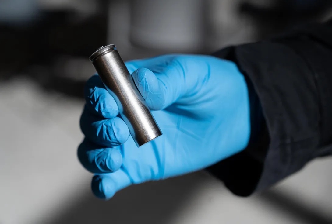

A new fabrication technique could allow solid-state automotive lithium-ion batteries to adopt nonflammable ceramic electrolytes using the same production processes as in batteries made with conventional liquid electrolytes.
The melt-infiltration technology developed by materials science researchers at the Georgia Institute of Technology uses electrolyte materials that can be infiltrated into porous yet densely packed, thermally stable electrodes. The one-step process produces high-density composites based on pressure-less, capillary-driven infiltration of a molten solid electrolyte into porous bodies, including multilayered electrode-separator stacks.
“While the melting point of traditional solid state electrolytes can range from 700 degrees Celsius to over 1,000 degrees Celsius, we operate at a much lower temperature range, depending on the electrolyte composition, roughly from 200 to 300 degrees Celsius,” explained Gleb Yushin, a professor in the School of Materials Science and Engineering at Georgia Tech. “At these lower temperatures, fabrication is much faster and easier. Materials at low temperatures don’t react. The standard electrode assemblies, including the polymer binder or glue, can be stable in these conditions.”
The new technique, to be reported March 8 in the journal Nature Materials, could allow large automotive Li-ion batteries to be made safer with 100% solid-state nonflammable ceramic rather than liquid electrolytes using the same manufacturing processes of conventional liquid electrolyte battery production. The patent-pending manufacturing technology mimics low-cost fabrication of commercial Li-ion cells with liquid electrolytes, but instead uses solid state electrolytes with low melting points that are melted and infiltrated into dense electrodes. As a result, high-quality multi-layered cells of any size or shape could be rapidly manufactured at scale using proven tools and processes developed and optimized over the last 30 years for Li-ion.
“Melt-infiltration technology is the key advance. The cycle life and stability of Li-ion batteries depend strongly on the operating conditions, particularly temperature,” Georgia Tech graduate student Yiran Xiao explained. “If batteries are overheated for a prolonged period, they commonly begin to degrade prematurely, and overheated batteries may catch on fire. That has prompted nearly all electric vehicles (EV) to include sophisticated and rather expensive cooling systems.” In contrast, solid-state batteries may only require heaters, which are significantly less expensive than cooling systems.
Yushin and Xiao are encouraged by the potential of this manufacturing process to enable battery makers to produce lighter, safer, and more energy-dense batteries.
“The developed melt-infiltration technology is compatible with a broad range of material chemistries, including so-called conversion-type electrodes. Such materials have been demonstrated to increase automotive cell energy density by over 20% now and by more than 100% in the future,” said co-author and Georgia Tech research scientist Kostiantyn Turcheniuk, noting that higher density cells support longer driving ranges. The cells need high-capacity electrodes for that performance leap.
Georgia Tech’s technique is not yet commercially ready, but Yushin predicts that if a significant portion of the future EV market embraces solid-state batteries, “This would probably be the only way to go,” since it will allow manufacturers to use their existing production facilities and infrastructure.
“That’s why we focused on this project – it was one of the most commercially viable areas of innovation for our lab to pursue,” he said.
Battery cell prices hit $100 per kilowatt hour for the first time in 2020. According to Yushin, they will need to drop below $70 per kilowatt hour before the consumer EV market can fully open. Battery innovation is critical to that occurring.
The Materials Science lab team currently is focused on developing other electrolytes that will have lower melting points and higher conductivities using the same technique proven in the lab.
Yushin envisions this research team’s manufacturing advance opening the floodgates to more innovation in this area.
“So many incredibly smart scientists are focused on solving very challenging scientific problems, while completely ignoring economic and technical practicality. They are studying and optimizing very high-temperature electrolytes that are not only dramatically more expensive to use in cells but are also up to five times heavier compared with liquid electrolytes,” he explained. “My goal is to push the research community to look outside that chemical box.”
In addition to Yushin, Xiao and Turcheniuk, co-authors included Aashray Narla, Ah-Young Song, Alexandre Magasinski, Ayush Jain, Sheirley Huang, and Haewon Lee from Georgia Tech, and Xiaolei Re from both Georgia Tech and Chongqing Technology and Business University in China.
This work was mostly supported by Sila Nanotechnologies Inc., a Georgia Tech startup, with characterization performed at the Materials Characterization Center at Georgia Tech. Any opinions, findings, and conclusions or recommendations expressed in this material are those of the authors and do not necessarily reflect the views of the sponsoring organization.
Gleb Yushin is co-founder, CTO, and a stockholder of Sila. Yushin is entitled to royalties derived from Sila’s sale of products related to the research described in this paper. This study could affect his personal financial status. The terms of this arrangement have been reviewed and approved by Georgia Tech in accordance with its conflict of interest policies.
CITATION: Y. Xiao, et al., “Electrolyte Melt-Infiltration for Scalable Manufacturing of Inorganic All-Solid-State Lithium-Ion Batteries.” (Nature Materials, 2021) https://dx.doi.org/10.1038/s41563-021-00943-2.
News Contact
Anne Wainscott-Sargent
Research News
(404-435-5784)