Jul. 30, 2024
From airplanes to soda cans, aluminum is a crucial — not to mention, an incredibly sustainable — material in manufacturing. Since 2019, Georgia Tech has partnered with Novelis, a global leader in aluminum rolling and recycling, through the Novelis Innovation Hub to advance research and business opportunities in aluminum manufacturing.
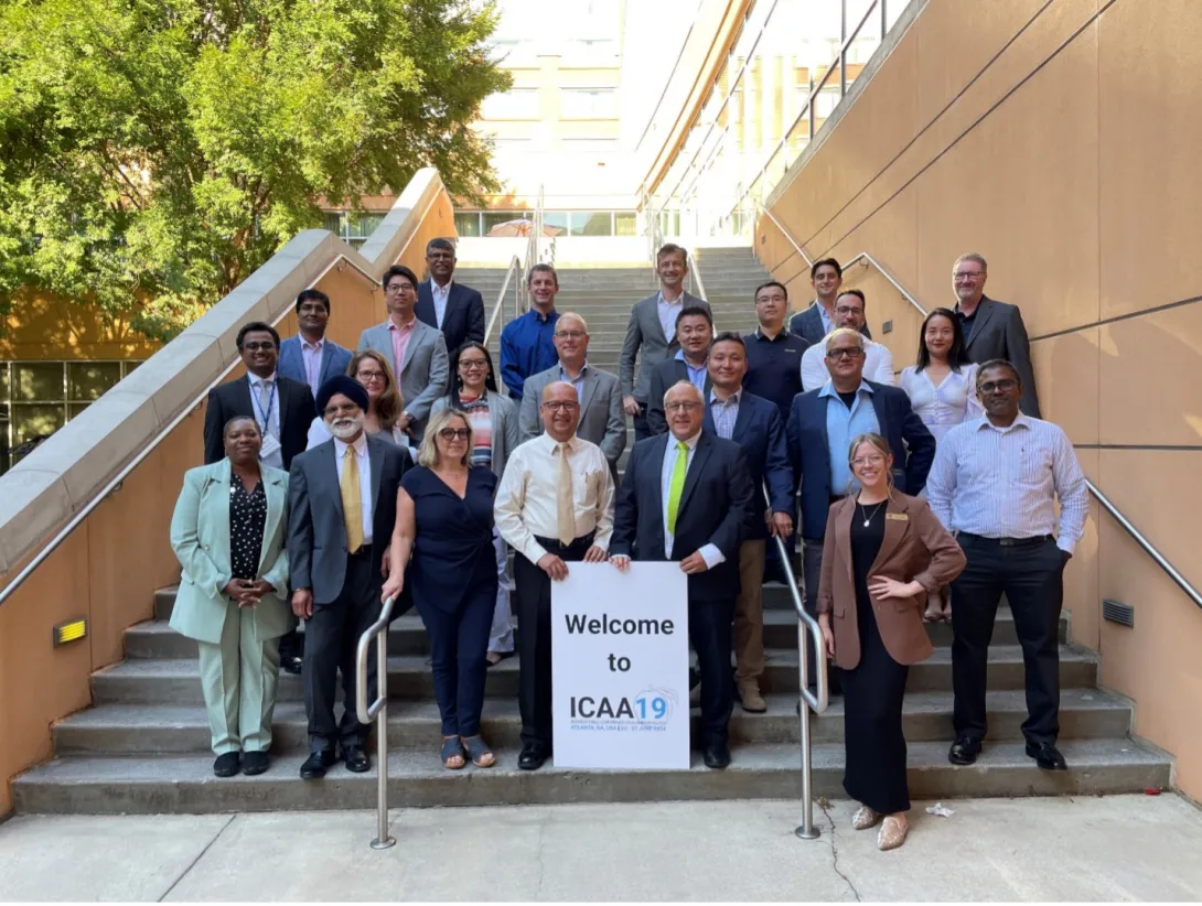
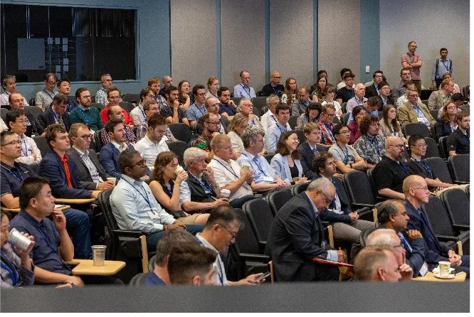
Novelis and the Georgia Institute of Technology recently co-hosted the 19th International Conference on Aluminum Alloys (ICAA19). Held on Georgia Tech's campus, this event brought together the brightest minds in aluminum technology for four days of intensive learning and networking.
Since its inception in 1986, ICAA has been the premier global forum for aluminum manufacturing innovations. This year, the conference attracted over 300 participants from 19 countries, including representatives from academia, research organizations, and industry leaders.
“The diverse mix of attendees created a rich tapestry of knowledge and experience, fostering a robust exchange of ideas,” said Naresh Thadhani, conference co-chair and professor in the School of Materials Science and Engineering
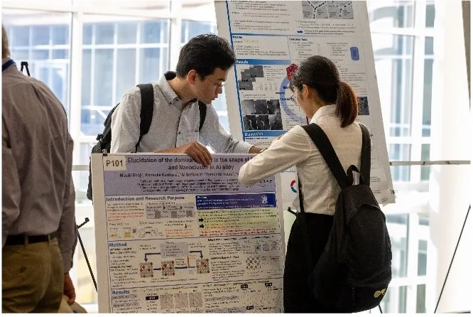
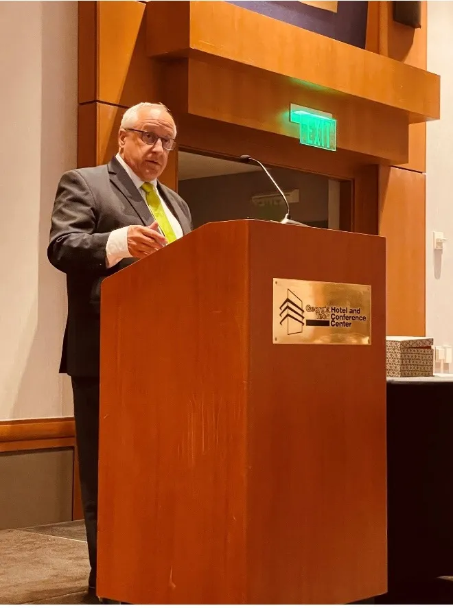
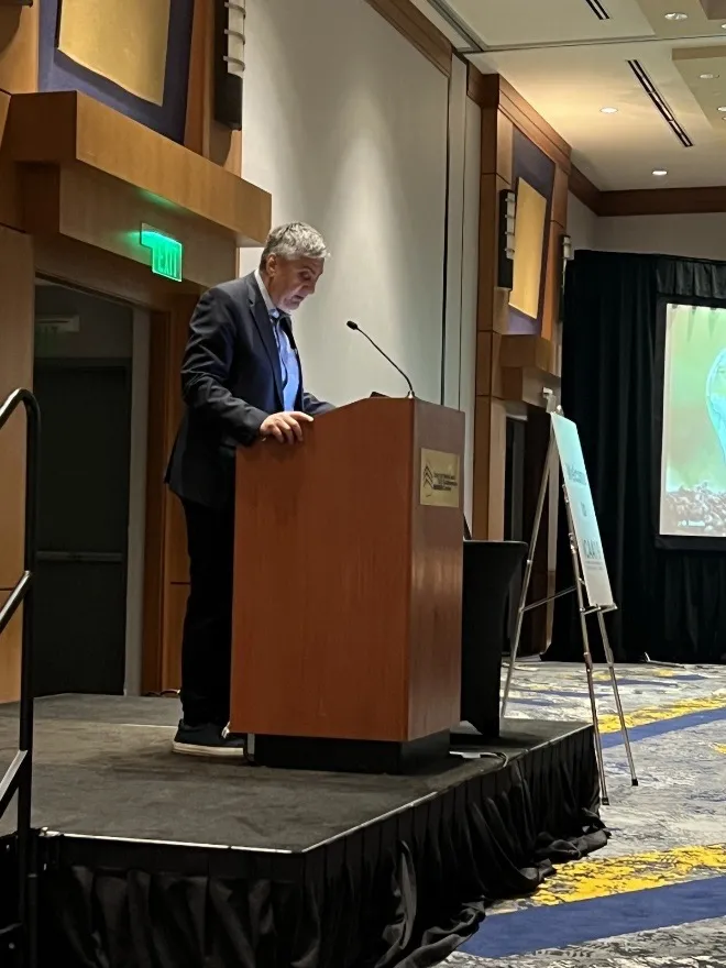
ICAA19 featured 12 symposia topics and over 250 technical presentations, delving into critical themes such as sustainability, future mobility, and next-generation manufacturing. Keynote addresses from leaders at the Aluminum Association, Airbus, and Coca-Cola set the stage for insightful discussions. Novelis Chief Technology Officer Philippe Meyer and Georgia Tech Executive Vice President for Research Chaouki Abdallah headlined the event, underscoring the importance of Novelis’ partnership with Georgia Tech.
Marking the fifth anniversary of the Novelis Innovation Hub at Georgia Tech, Hub Executive Director Shreyes Melkote says that “ICAA19 represents a prime example of the close collaboration between Novelis and the Institute, enabled by the Novelis Innovation Hub.” Melkote, a professor in the George W. Woodruff School of Mechanical Engineering, also serves as the associate director of the Georgia Tech Manufacturing Institute.
“This unique center for research, development, and technology has been instrumental in advancing aluminum innovations, exemplifying the power of partnerships in driving industry progress,” says Meyer. “As we reflect on the success of ICAA19, we remain committed to strengthening our existing partnerships and forging new alliances to accelerate innovation. The collaborative spirit showcased at the conference is a testament to our dedication to leading the aluminum industry into a more sustainable future.”
News Contact
Audra Davidson
Research Communications Program Manager
Georgia Tech Manufacturing Institute
Jul. 30, 2024
Timothy Lieuwen has been appointed interim executive vice president for Research (EVPR) by Georgia Tech President Ángel Cabrera, effective September 10.
Lieuwen is a Regents’ Professor, the David S. Lewis, Jr. Chair in the Daniel Guggenheim School of Aerospace Engineering, and executive director of the Strategic Energy Institute. His research interests range from clean energy and propulsion systems to energy policy, national security, and regional economic development. He works closely with industry and government to address fundamental problems and identify solutions in the development of clean energy systems and alternative fuels.
A proud Georgia Tech alumnus, Lieuwen (M.S. ME 1997, Ph.D. ME 1999) has had a remarkable academic career. He is a member of the National Academy of Engineering and is a fellow of the American Society of Mechanical Engineers, the American Institute of Aeronautics and Astronautics, the American Physical Society, the Combustion Institute, and the Indian National Academy of Engineering (foreign fellow). He has received numerous awards, including the ASME George Westinghouse Gold Medal and the AIAA Pendray Award. He serves on governing or advisory boards of three Department of Energy national labs: Oak Ridge National Laboratory, Pacific Northwest National Laboratory, and the National Renewable Energy Laboratory and was appointed by the U.S. Secretary of Energy to the National Petroleum Council.
Lieuwen has authored or edited four books on combustion and over 400 scientific publications. He also holds nine patents, several of which are licensed to industry, and is founder of an energy analytics company, Turbine Logic, where he acts as chief technology officer.
In Lieuwen’s appointment announcement, President Cabrera said, “Tim’s extensive experience and knowledge of Georgia Tech makes him uniquely suited to lead our research enterprise as we search for a permanent EVPR. I am grateful for his willingness to serve the Institute during this period of remarkable growth, and I look forward to working with him and the rest of the team.”
News Contact
Shelley Wunder-Smith
Director of Research Communications
Jul. 23, 2024
When it comes to manufacturing innovation, the “valley of death” — the gap between the lab and the industry floor where even the best discoveries often get lost — looms large.
“An individual faculty’s lab focuses on showing the innovation or the new science that they discovered,” said Aaron Stebner, professor and Eugene C. Gwaltney Jr. Chair in Manufacturing in the George W. Woodruff School of Mechanical Engineering. “At that point, the business case hasn't been made for the technology yet — there's no testing on an industrial system to know if it breaks or if it scales up. A lot of innovation and scientific discovery dies there.”
The Georgia Tech Manufacturing Institute (GTMI) launched the Advanced Manufacturing Pilot Facility (AMPF) in 2017 to help bridge that gap.
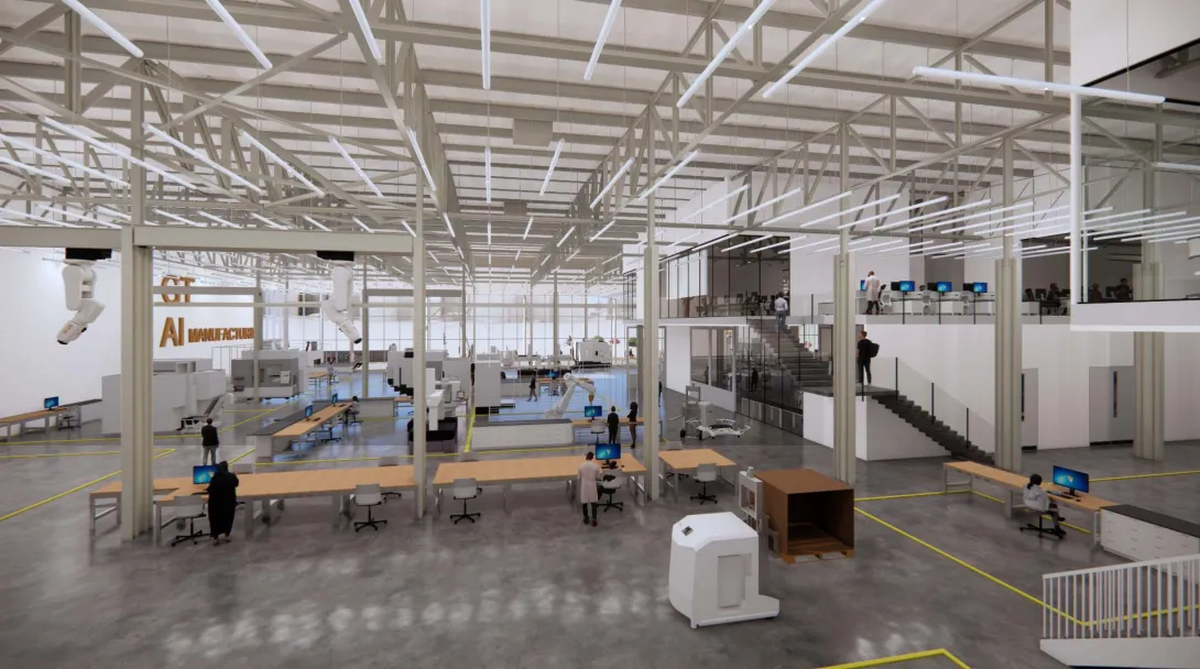
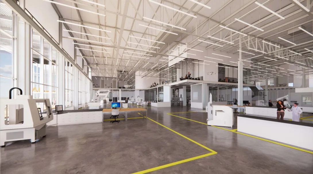
Now, GTMI is breaking ground on an extensive expansion to bring new capabilities in automation, artificial intelligence, and data management to the facility.
“This will be the first facility of this size that's being intentionally designed to enable AI to perform research and development in materials and manufacturing at the same time,” said Stebner, “setting up GTMI as not just a leader in Georgia, but a leader in automation and AI in manufacturing across the country.”
AMPF: A Catalyst for Collaboration
Located just north of Georgia Tech’s main campus, APMF is a 20,000-square-foot facility serving as a teaching laboratory, technology test bed, and workforce development space for manufacturing innovations.
“The pilot facility,” says Stebner, “is meant to be a place where stakeholders in academic research, government, industry, and workforce development can come together and develop both the workforce that is needed for future technologies, as well as mature, de-risk, and develop business cases for new technologies — proving them out to the point where it makes sense for industry to pick them up.”
In addition to serving as the flagship facility for GTMI research and the state’s Georgia AIM (Artificial Intelligence in Manufacturing) project, the AMPF is a user facility accessible to Georgia Tech’s industry partners as well as the Institute’s faculty, staff, and students.
“We have all kinds of great capabilities and technologies, plus staff that can train students, postdocs, and faculty on how to use them,” said Stebner, who also serves as co-director of the GTMI-affiliated Georgia AIM project. “It creates a unique asset for Georgia Tech faculty, staff, and students.”
Bringing AI and Automation to the Forefront
The renovation of APMF is a key component of the $65 million grant, awarded to Georgia Tech by the U.S. Department of Commerce’s Economic Development Administration in 2022, which gave rise to the Georgia AIM project. With over $23 million in support from Georgia AIM, the improved facility will feature new workforce training programs, personnel, and equipment.
Set to complete in Spring 2026, the Institute’s investment of $16 million supports construction that will roughly triple the size of the facility — and work to address a major roadblock for incorporating AI and automation into manufacturing practices: data.
“There’s a lot of work going on across the world in using machine learning in engineering problems, including manufacturing, but it's limited in scale-up and commercial adoption,” explained Stebner.
Machine learning algorithms have the potential to make manufacturing more efficient, but they need a lot of reliable, repeatable data about the processes and materials involved to be effective. Collecting that data manually is monotonous, costly, and time-consuming.
“The idea is to automate those functions that we need to enable AI and machine learning” in manufacturing, says Stebner. “Let it be a facility where you can imagine new things and push new boundaries and not just be stuck in demonstrating concepts over and over again.”
To make that possible, the expanded facility will couple AI and data management with robotic automation.
“We're going to be able to demonstrate automation from the very beginning of our process all the way through the entire ecosystem of manufacturing,” said Steven Sheffield, GTMI’s senior assistant director of research operations.
“This expansion — no one else has done anything like it,” added Steven Ferguson, principal research scientist with GTMI and managing director of Georgia AIM. “We will have the leading facility for demonstrating what a hyperconnected and AI-driven manufacturing enterprise looks like. We’re setting the stage for Georgia Tech to continue to lead in the manufacturing space for the next decade and beyond.”
News Contact
Audra Davidson
Research Communications Program Manager
Georgia Tech Manufacturing Institute
Jul. 23, 2024
From keeping warm in the winter to doing laundry, heat is crucial to daily life. But as the world grapples with climate change, buildings’ increasing energy consumption is a critical problem. Currently, heat is produced by burning fossil fuels like coal, oil, and gas, but that will need to change as the world shifts to clean energy.
Georgia Tech researchers in the George W. Woodruff School of Mechanical Engineering (ME) are developing more efficient heating systems that don’t rely on fossil fuels. They demonstrated that combining two commonly found salts could help store clean energy as heat; this can be used for heating buildings or integrated with a heat pump for cooling buildings.
The researchers presented their research in “Thermochemical Energy Storage Using Salt Mixtures With Improved Hydration Kinetics and Cycling Stability,” in the Journal of Energy Storage.
Reaction Redux
The fundamental mechanics of heat storage are simple and can be achieved through many methods. A basic reversible chemical reaction is the foundation for their approach: A forward reaction absorbs heat and then stores it, while a reverse reaction releases the heat, enabling a building to use it.
ME Assistant Professor Akanksha Menon has been interested in thermal energy storage since she began working on her Ph.D. When she arrived at Georgia Tech and started the Water-Energy Research Lab (WERL), she became involved in not only developing storage technology and materials but also figuring out how to integrate them within a building. She thought understanding the fundamental material challenges could translate into creating better storage.
“I realized there are so many things that we don't understand, at a scientific level, about how these thermo-chemical materials work between the forward and reverse reactions,” she said.
The Superior Salt
The reactions Menon works with use salt. Each salt molecule can hold a certain number of water molecules within its structure. To instigate the chemical reaction, the researchers dehydrate the salt with heat, so it expels water vapor as a gas. To reverse the reaction, they hydrate the salt with water, forcing the salt structure’s expansion to accommodate those water molecules.
It sounds like a simple process, but as this expansion/contraction process happens, the salt gets more stressed and will eventually mechanically fail, the same way lithium-ion batteries only have so many charge-discharge cycles.
“You can start with something that's a nice spherical particle, but after it goes through a few of these dehydration-hydration cycles, it just breaks apart into tiny particles and completely pulverizes or it overhydrates and agglomerates into a block,” Menon explained.
These changes aren’t necessarily catastrophic, but they do make the salt ineffective for long-term heat storage as the storage capacity decreases over time.
Menon and her student, Erik Barbosa, a Ph.D. student in ME, began combining salts that react with water in different ways. After testing six salts over two years, they found two that complemented each other well. Magnesium chloride often fails because it absorbs too much water, whereas strontium chloride is very slow to hydrate. Together, their respective limitations can mutually benefit each other and lead to improved heat storage.
“We didn't plan to mix salts; it was just one of the experiments we tried,” Menon said. “Then we saw this interactive behavior and spent a whole year trying to understand why this was happening and if it was something we could generalize to use for thermal energy storage.”
The Energy Storage of the Future
Menon is just beginning with this research, which was supported by a National Science Foundation (NSF) CAREER Award. Her next step is developing the structures capable of containing these salts for heat storage, which is the focus of an Energy Earthshots project funded by the U.S. Department of Energy’s (DOE) Office of Basic Energy Sciences.
A system-level demonstration is also planned, where one solution is filling a drum with salts in a packed bed reactor. Then hot air would flow across the salts, dehydrating them and effectively charging the drum like a battery. To release that stored energy, humid air would be blown over the salts to rehydrate the crystals. The subsequently released heat can be used in a building instead of fossil fuels. While initiating the reaction needs electricity, this could come from off-peak (excess renewable electricity) and the stored thermal energy could be deployed at peak times. This is the focus of another ongoing project in the lab that is funded by the DOE’s Building Technologies Office.
Ultimately, this technology could lead to climate-friendly energy solutions. Plus, unlike many alternatives like lithium batteries, salt is a widely available and cost-effective material, meaning its implementation could be swift. Salt-based thermal energy storage can help reduce carbon emissions, a vital strategy in the fight against climate change.
“Our research spans the range from fundamental science to applied engineering thanks to funding from the NSF and DOE,” Menon said. “This positions Georgia Tech to make a significant impact toward decarbonizing heat and enabling a renewable future.”
News Contact
Tess Malone, Senior Research Writer/Editor
tess.malone@gatech.edu
Jul. 19, 2024
When Blair Brettmann was a sophomore at the University of Texas at Austin, her advisor told her about the National Science Foundation’s Research Experience for Undergraduates (REU) program. The summer program enables undergraduates to conduct research at top institutions across the country. Brettmann spent the summer of 2005 at Cornell working in a national nanotechnology program — a defining experience that led to her current research in molecular engineering for integrated product development.
“I didn't know for sure if I wanted to attend grad school until after the REU experience,” Brettmann said. “Through it, I went to high-level seminars for the first time, and working in a cleanroom was super cool.”
Her experience was so positive that the following summer, Brettmann completed a second REU at the Massachusetts Institute of Technology, where she eventually earned her Ph.D. Now an associate professor in Georgia Tech’s School of Chemical and Biomolecular Engineering and School of Materials Science and Engineering and an Institute for Matter and Systems faculty member, Brettmann is an REU mentor for the current iteration of the nanotechnology program — now taking place at Georgia Tech.
Brettmann’s mentee this summer, Marissa Moore, is having a similarly positive experience. A rising senior in chemical engineering at the University of Missouri-Columbia (Mizzou), Moore was already familiar with Georgia Tech because her father received his chemical engineering Ph.D. from the Institute; she hopes to do the same. Her passion for research began as she grew up with her sister, who had cerebral palsy and epilepsy.
“We spent a lot of time in hospitals trying out new devices and looking for different medications that would help her, so I knew I wanted to make a difference in this area,” she said.
But Moore wasn’t interested in being a doctor. Instead, she wanted to develop the materials that could be a solution for someone like her sister. Her undergraduate research focuses on materials and biomaterials for medical applications, and Georgia Tech is enabling her to deep-dive into pure materials science.
“What I'm working on at both universities is biodegradable polymers, but at Mizzou I’m developing that polymer from the ground up, and at Tech I’m using the properties of the polymer and finding how to make them,” she explained.
Having the opportunity to work in nanotechnology through the Institute for Materials and use Georgia Tech’s famous cleanroom made this REU stand out for Moore.
“I had never been in the cleanroom before, so that was one of the most eye-opening experiences,” she said. “It was cool to gown up and learn all of the safety precautions.”
For Brettmann, hands-on research experiences like this make the REU program unique — and crucial — for potential graduate students.
“Having your experiments fail, or even having things not turn out as you expect them to is an important part of the graduate research experience,” she said. “One of the best things about REU is it can be a first experience for people and help them decide what to do in grad school later on.”
News Contact
Tess Malone, Senior Research Writer/Editor
tess.malone@gatech.edu
Jul. 19, 2024
Every millisecond will matter when the world's best athletes gather in Paris for the Summer Olympics, and track and field athletes will compete on a surface designed to produce record-breaking performances.
Mondo athletic tracks have been underneath the feet of Olympians since 1972. In that time, 300 records were broken on surfaces designed and constructed in Alba, Italy, including 15 at the Centennial Olympic Games in Atlanta.
Consistency Is Key
Georgia Tech’s George C. Griffin Track and Field Facility was outfitted with a Mondo track before the 1996 Games to serve as the workout track for the Olympic Village, and the material has been a staple at the facility ever since. Yellow Jacket Track and Field Coach Grover Hinsdale, a coach to three Olympic gold medalists, explains that the consistency in Mondo's construction sets it apart from all other tracks.
"A Mondo track is made in a climate-controlled factory, processed from the raw rubber to the finished product. So, every square inch of Mondo is the same — same durometer, same thickness, everything is the same. All other rubberized track surfaces are poured on-site, so variables like temperature and humidity affect the result, and you may end up with lanes that don't set uniformly,” he said.
Hinsdale likened the installation process to laying carpet. It will take more than 2,800 glue pots to set the 13,000 square meters of track inside Stade de France. Jud Ready, a principal research engineer in the School of Materials Science and Engineering, says the evolution of the company’s technology has also contributed to producing faster tracks.
"They're able to alter the rubber track's energy return mechanism by changing the shape of the particulate and the compressibility of it," Ready said. "Longevity is less of a concern for the Paris track, so they can tune it to emphasize speed."
Maximizing Performance
Each layer of the track surface plays a different role in helping athletes achieve peak performance. Hinsdale describes how those layers come together with each step.
"When your foot strikes down on an asphalt surface or you're running down a sidewalk, there's virtually no give other than what's taking place in the muscles and joints of your body. The surface is giving nothing back. When your foot strikes a Mondo surface, it'll sink in slightly, and the surface gives energy back. This pushes your foot back off that track quicker, putting the foot back into the cycle to complete another stride,” he said.
Because of the energy given back by the thin and firm surface of the Mondo track, Hinsdale says, sprinters and distance runners will run faster with the same effort they normally exert on any other surface.
Athletes look for every edge to get ahead of the competition. Ready's course, Materials Science and Engineering of Sports, examines how that advantage can be found at the scientific level.
"All sports are so heavily driven by material advancements these days,” he said. “Yes, we use the mechanical properties we've used since the Egyptians started racing chariots, but as material scientists, we keep trying to make things better.”
Viewers will notice the unique purple hue of the Paris track when the games begin, but Ready and Hinsdale don't expect the striking color to affect performance.
News Contact
Steven Gagliano - Institute Communications
Jul. 16, 2024
Georgia Tech will lead a consortium of 12 universities and 12 national labs as part of a $25 million U.S. Department of Energy National Nuclear Security Administration (NNSA) award. This is the second time Georgia Tech has won this award and led research and development efforts to aid NNSA’s nonproliferation, nuclear science, and security endeavors.
The Consortium for Enabling Technologies and Innovation (ETI) 2.0 will leverage the strong foundation of interdisciplinary, collaboration-driven technological innovation developed in the ETI Consortium funded in 2019. The technical mission of the ETI 2.0 team is to advance technologies across three core disciplines: data science and digital technologies in nuclear security and nonproliferation, precision environmental analysis for enhanced nuclear nonproliferation vigilance and emergency response, and emerging technologies. They will be advanced by research projects in novel radiation detectors, algorithms, testbeds, and digital twins.
“What we're trying to do is bring those emergent technologies that are not implemented right now to fruition,” said Anna Erickson, Woodruff Professor and associate chair for research in the George W. Woodruff School of Mechanical Engineering, who leads both grants. “We want to understand what's ahead in the future for both the technology and the threats, which will help us determine how we can address it today.”
While half the original collaborators remain, Erickson sought new institutional partners for their research expertise, including Abilene Christian University, University of Alaska Fairbanks, Stony Brook University, Rensselaer Polytechnic Institute, and Virginia Commonwealth University. Other university collaborators include the Colorado School of Mines, the Massachusetts Institute of Technology, Ohio State University, Texas A&M University, the University of Texas at Austin, and the University of Wisconsin–Madison.
National lab partners are the Argonne National Laboratory, Brookhaven National Laboratory, Idaho National Laboratory, Lawrence Berkeley National Laboratory, Lawrence Livermore National Laboratory, Los Alamos National Laboratory, Nevada National Security Site, Oak Ridge National Laboratory, Pacific Northwest National Laboratory, Princeton Plasma Physics Laboratory, Sandia National Laboratories, and Savannah River National Laboratory.
The partners, along with the other NNSA Consortia, gathered at Texas A&M in June to present the new results of the research — NNSA DNN R&D University Program Review — and the kickoff will be hosted in Atlanta in February 2025. More than 300 collaborators, including 150 students, met for four days to share their research and develop new partnerships.
Engaging students in research in the nuclear nonproliferation field is a key part of the award. The plan is to train over 50 graduate students, provide internships for graduate and undergraduate students, and offer faculty-student lab visit fellowships. This pipeline aims to develop well-rounded professionals equipped with the expertise to tackle future nonproliferation challenges.
“Because nuclear proliferation is a multifaceted problem, we try to bring together people from outside nuclear engineering to have a conversation about the problems and solutions,” Erickson said.
“One of the biggest accomplishments of ETI 1.0 is this incredible relationship that our university PIs have been able to forge with national labs,” she said. “Over five years, we've supported over 70 student internships at national labs, and we have already transitioned a number of Ph.D. students to careers at national labs.”
As the consortium efforts continue, the team looks forward to the next phase of engagement with government, university, and national lab partners.
“With a united team and a focus on cutting-edge technologies, the ETI 2.0 consortium is poised to break new ground in nuclear nonproliferation,” Erickson said. “Collaboration is the fuel, and innovation is the engine.”
News Contact
Tess Malone, Senior Research Writer/Editor
tess.malone@gatech.edu
Jul. 15, 2024
Time is winding down on Olympic organizers’ plans to stage open-water swimming events in Paris’ iconic Seine River later this month. The city spent $1.5 billion on new infrastructure to clean up the Seine, yet water samples continue to show high levels of potentially toxic E. coli.
The river has been closed to swimmers for the past 100 years because of pollution, but Olympic organizers hope to stage the triathlon and marathon swimming events in the water flowing in the shadow of the Eiffel Tower.
Katherine Graham has followed the saga in Paris. She’s an assistant professor in the Georgia Tech School of Civil and Environmental Engineering who studies the fate and transport of pathogens and their indicators in water, including E. coli. She said several factors are at play in the Seine.
“Paris, like most large cities, has a lot of concrete and not much dirt and grass for water to soak into."
Read the entire story on the College of Engineering website.
News Contact
Jason Maderer
College of Engineering
maderer@gatech.edu
Jun. 12, 2024
Adoptive T-cell therapy has revolutionized medicine. A patient’s T-cells — a type of white blood cell that is part of the body’s immune system — are extracted and modified in a lab and then infused back into the body, to seek and destroy infection, or cancer cells.
Now Georgia Tech bioengineer Ankur Singh and his research team have developed a method to improve this pioneering immunotherapy.
Their solution involves using nanowires to deliver therapeutic miRNA to T-cells. This new modification process retains the cells’ naïve state, which means they’ll be even better disease fighters when they’re infused back into a patient.
“By delivering miRNA in naïve T cells, we have basically prepared an infantry, ready to deploy,” Singh said. “And when these naïve cells are stimulated and activated in the presence of disease, it’s like they’ve been converted into samurais.”
Lean and Mean
Currently in adoptive T-cell therapy, the cells become stimulated and preactivated in the lab when they are modified, losing their naïve state. Singh’s new technique overcomes this limitation. The approach is described in a new study published in the journal Nature Nanotechnology.
“Naïve T-cells are more useful for immunotherapy because they have not yet been preactivated, which means they can be more easily manipulated to adopt desired therapeutic functions,” said Singh, the Carl Ring Family Professor in the Woodruff School of Mechanical Engineering and the Wallace H. Coulter Department of Biomedical Engineering.
The raw recruits of the immune system, naïve T-cells are white blood cells that haven’t been tested in battle yet. But these cellular recruits are robust, impressionable, and adaptable — ready and eager for programming.
“This process creates a well-programmed naïve T-cell ideal for enhancing immune responses against specific targets, such as tumors or pathogens,” said Singh.
The precise programming naïve T-cells receive sets the foundational stage for a more successful disease fighting future, as compared to preactivated cells.
Giving Fighter Cells a Boost
Within the body, naïve T-cells become activated when they receive a danger signal from antigens, which are part of disease-causing pathogens, but they send a signal to T-cells that activate the immune system.
Adoptive T-cell therapy is used against aggressive diseases that overwhelm the body’s defense system. Scientists give the patient’s T-cells a therapeutic boost in the lab, loading them up with additional medicine and chemically preactivating them.
That’s when the cells lose their naïve state. When infused back into the patient, these modified T-cells are an effective infantry against disease — but they are prone to becoming exhausted. They aren’t samurai. Naïve T-cells, though, being the young, programmable recruits that they are, could be.
The question for Singh and his team was: How do we give cells that therapeutic boost without preactivating them, thereby losing that pristine, highly suggestable naïve state? Their answer: Nanowires.
NanoPrecision: The Pointed Solution
Singh wanted to enhance naïve T-cells with a dose of miRNA. miRNA is a molecule that, when used as a therapeutic, works as a kind of volume knob for genes, turning their activity up or down to keep infection and cancer in check. The miRNA for this study was developed in part by the study’s co-author, Andrew Grimson of Cornell University.
“If we could find a way to forcibly enter the cells without damaging them, we could achieve our goal to deliver the miRNA into naïve T cells without preactivating them,” Singh explained.
Traditional modification in the lab involves binding immune receptors to T-cells, enabling the uptake of miRNA or any genetic material (which results in loss of the naïve state). “But nanowires do not engage receptors and thus do not activate cells, so they retain their naïve state,” Singh said.
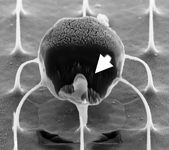
The nanowires, silicon wafers made with specialized tools at Georgia Tech’s Institute for Electronics and Nanotechnology, form a fine needle bed. Cells are placed on the nanowires, which easily penetrate the cells and deliver their miRNA over several hours. Then the cells with miRNA are flushed out from the tops of the nanowires, activated, eventually infused back into the patient. These programmed cells can kill enemies efficiently over an extended time period.
“We believe this approach will be a real gamechanger for adoptive immunotherapies, because we now have the ability to produce T-cells with predictable fates,” says Brian Rudd, a professor of immunology at Cornell University, and co-senior author of the study with Singh.
The researchers tested their work in two separate infectious disease animal models at Cornell for this study, and Singh described the results as “a robust performance in infection control.”
In the next phase of study, the researchers will up the ante, moving from infectious disease to test their cellular super soldiers against cancer and move toward translation to the clinical setting. New funding from the Georgia Clinical & Translational Science Alliance is supporting Singh’s research.
CITATION: Kristel J. Yee Mon, Sungwoong Kim, Zhonghao Dai, Jessica D. West, Hongya Zhu5, Ritika Jain, Andrew Grimson, Brian D. Rudd, Ankur Singh. “Functionalized nanowires for miRNA-mediated therapeutic programming of naïve T cells,” Nature Nanotechnology.
FUNDING: Curci Foundation, NSF (EEC-1648035, ECCS-2025462, ECCS-1542081), NIH (5R01AI132738-06, 1R01CA266052-01, 1R01CA238745-01A1, U01CA280984-01, R01AI110613 and U01AI131348).
News Contact
Jerry Grillo
Jun. 07, 2024
Nakia Melecio, the VentureLab Principal under the Office of Commercialization, has made remarkable progress in enhancing the grant programs of the National Institutes of Health (NIH). Over an intensive eight-month period, Melecio was part of an evaluation committee that focused on refining initiatives of the NIH’s National Cancer Institute, particularly the Small Business Transition Grant and other related grant programs.
“The experience was both enlightening and challenging,” Melecio said. “We engaged with faculty from over 20 universities to understand the diverse needs — from early-stage research to the commercialization of technology.” His pivotal role in streamlining the application processes for the Small Business Innovation Research and Small Business Technology Transfer programs has significantly enhanced their efficiency and accessibility.
A key aspect of Melecio’s efforts was to increase participation from historically underrepresented groups, with a significant focus on supporting historically Black colleges and universities and minority-serving institutions. His strategic insights have helped reshape these programs to better facilitate the commercialization of technologies developed within academic institutions.
Keith McGreggor, director of VentureLab, praised Melecio’s contributions. “Nakia’s work embodies our mission to transform research into viable market opportunities, ensuring broad access and benefit. The approval of the committee’s recommendations by the NCI leadership marks a significant advancement in our ongoing effort to make NIH funding more accessible and effective,” he said.
As these enhancements are implemented, they promise to significantly improve the landscape for commercializing technologies originating from university research, fostering broader innovation and practical application of groundbreaking discoveries.
The Office of Commercialization at Georgia Tech continues to support faculty and researchers as they navigate these improved opportunities, ensuring that the leadership and expertise within our community are directed toward national and global advancements in science and technology.
Stay engaged with the Office of Commercialization for ongoing updates on this and other initiatives.
News Contact
Lacey Cameron
Pagination
- Previous page
- 12 Page 12
- Next page
