Jul. 16, 2024

What makes a swimming pool fast? It’s not just the fit, strong, and elite athletes competing at the Summer Olympics in Paris. The speed of swimming is also created by the structural engineering and materials used at the venue.
In the United States, there’s no greater example than Georgia Tech’s McAuley Aquatic Center, which hosted the Olympics in Atlanta 28 years ago. The pool continues to be one of the fastest in the world and will host the NCAA Division I men’s and women’s national championships this coming March.
Everything — air flow, depth, and more — are in place with speed in mind.
“There are three primary reasons why the Georgia Tech pool is still among the fastest, even after a quarter century,” said Jud Ready, an adjunct professor in the School of Materials Science and Engineering who teaches a class about the materials and engineering concepts of sports. “Two are at the bottom of the pool and the other is at the sides.”
News Contact
Jason Maderer
College of Engineering
May. 30, 2024
Semiconductors make our world run, but the industry faces a turning point. For decades, computer chip efficiency has doubled every two years, but that progress is slowing. To complicate the problem further, global demand for semiconductors threatens to outpace the supply. The U.S. has the opportunity to meet the growing need for chips — both by increasing domestic manufacturing and building up the workforce, which is at its lowest in decades. To bolster semiconductor research and manufacturing, in 2022, Congress passed the $52.7 billion bipartisan CHIPS and Science Act that President Joe Biden signed into law. New paradigms and pioneers are needed to make these critical advances.
Georgia Tech is playing a significant role in creating the next generation of chips, as the Institute is especially well positioned to innovate in the semiconductor field. All areas of the semiconductor stack — the components that build a chip, from hardware to artificial intelligence — are studied at Tech, and collaboration among faculty is a hallmark of its research enterprise. Such cooperation is necessary to build better chips, since they need to be reinvented in every layer of the stack.
News Contact
Media Contact: Tess Malone | tess.malone@gatech.edu
May. 29, 2024
Georgia Tech has been selected as one of six universities globally to receive funding for the newly established Global Industrial Technology Cooperation Center. The announcement was made by the Ministry of Trade, Industry, and Energy in South Korea during the Global Open Innovation Strategy Meeting in April.
The KIAT-Georgia Tech Semiconductor Electronics Center will receive $1.8 million to establish a sustainable semiconductor electronics research partnership between Korean companies, researchers, and Georgia Tech.
“I am thrilled to announce that we have secured funding to launch a groundbreaking collaboration between Georgia Tech’s world-class researchers and Korean companies,” said Hong Yeo, associate professor and Woodruff Faculty Fellow in the George W. Woodruff School of Mechanical Engineering and the Wallace H. Coulter Department of Biomedical Engineering. “This initiative will drive the development of cutting-edge technologies to advance semiconductor, sensors, and electronics research.”
Yeo will lead the center, and Michael Filler, interim executive director for the Institute of Electronics and Nanotechnology, and Muhannad Bakir, director of the 3D Advanced Packaging Research Center, will serve as co-PIs.
The center will focus on advancing semiconductor research, a critical area of technology that forms the backbone of modern electronics.
The Cooperation Center is a global technology collaboration platform designed to facilitate international joint research and development planning, partner matching, and local support for domestic researchers. The selection of Georgia Tech underscores the Institute’s leadership and expertise in the field of semiconductors.
News Contact
Amelia Neumeister
Research Communications Program Manager
May. 23, 2024

The Biden-Harris Administration announced that the U.S. Department of Commerce and Absolics, an affiliate of the Korea-based SKC, have signed a non-binding preliminary memorandum of terms to provide up to $75 million in direct funding under the CHIPS and Science Act to help advance U.S. technology leadership. The proposed investment would support the construction of a 120,000 square-foot facility in Covington, Georgia and the development of substrates technology for use in semiconductor advanced packaging. Started through a collaboration with the 3D Packaging Research Center at Georgia Tech, Absolics’ project serves as an example of American lab-to-fab development and production.
"Glass-core packaging holds the promise to revolutionize the field of advanced packaging and impact major paradigms such as artificial intelligence, mm-wave/THz communication, and photonic connectivity," said Muhannad Bakir, Dan Fielder Professor in the School of Electrical and Computer Engineering and Director of the 3D Systems Packaging Research Center at Georgia Tech. "We look forward to supporting Absolics in establishing a glass-core packaging facility in the State of Georgia through workforce development initiatives."
Because of President Biden’s CHIPS and Science Act, this proposed investment would support over an estimated 1,000 construction jobs and approximately 200 manufacturing and R&D jobs in Covington and enhance innovation capacity at Georgia Institute of Technology, supporting the local semiconductor talent pipeline.
The proposed investment with Absolics is the first proposed CHIPS investment in a commercial facility supporting the semiconductor supply chain by manufacturing a new advanced material.
News Contact
Amelia Neumeister
Research Communications Program Manager
May. 02, 2024
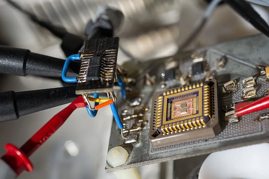
When Amy Bonecutter-Leonard was a second-semester undergraduate at the Georgia Institute of Technology, she applied for a work-study job in the cleanroom at the Microelectronics Research Center (MiRC). There, she learned process techniques for making the same type of electronic chips used in cellphones.
With this new knowledge, she could train and help other students with their research. At the time, Bonecutter-Leonard was a chemical engineering major with no plans to go into microelectronics. Working in the cleanroom changed that.
“I fell in love with microelectronics through exposure to the research and development work performed in the cleanroom,” she said.
What started as a student job led to her taking microelectronics classes — and eventually to a career in the field. “My work-study prepared me with hands-on technical skills I would have never learned from just being in a classroom,” she said. Now, Bonecutter-Leonard works as a microelectronics business chief engineer at defense contractor L3Harris Technologies.
Her story is one of many from the Institute for Electronics and Nanotechnology (IEN, the successor to MiRC), which has been training students from kindergarten to graduate school to be leaders in the microelectronics and nanotechnology space. The goal of IEN’s outreach is to make nanotechnology and microelectronics — such as computer chips and sensors — as accessible as any other science. Ultimately, these efforts will build up the U.S. workforce in the field, ensuring the country remains at the forefront of the technology that powers Americans’ everyday lives.
Building the Workforce
Bolstering the number of workers in the microelectronics industry is imperative to keep the U.S. globally competitive. Right now, 40% of the industry's labor force is older than 50, with practitioners aging out of their careers at a pace new talent cannot match. Additionally, heavy educational barriers to entry, including required degrees and specialized training, prevent more people from pursuing careers in the field. Without dedicated efforts, the entire sector — and the nation — will fall behind.
IEN is working to solve this pipeline problem.
“With the national semiconductor workforce aging, it is important now more than ever that we educate the next generation to move into these jobs,” said Michael Filler, IEN’s interim executive director. “IEN is proud to support the semiconductor industry by providing students with the interdisciplinary skills and hands-on technical training essential for success in this fast-paced, global field.”
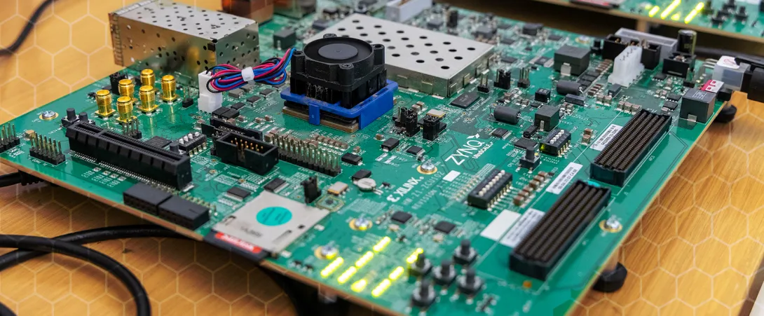
Georgia Tech is uniquely positioned to lead this charge with its 28,500 square feet of academic cleanroom space, the largest in the Southeast and among the largest in the U.S. From micro-electro-mechanical systems to electronics fabrication, workers have 100 bays in which to conduct leading-edge research. These cleanrooms are also key teaching and training facilities.
IEN invites anyone from around the world, whether affiliated with the Institute or not, to become a core user of the cleanroom facilities. The center also regularly hosts short courses for external partners — academic, industry, and government — in microfabrication and soft lithography for microfluidics. Over the past three years, more than 700 people went through new-user orientation, and 193 enrolled in the short courses.
Teaching the Next Generation
Making nanotechnology — of which microelectronics is an example — educationally accessible begins before college. Each semester, more than 800 K-12 students participate in IEN’s Introduction to Nanotechnology virtual lesson. Associate Director for Education and Outreach Mikkel Thomas begins his presentations by asking a simple question: What do you know about nanotechnology?
“About 99% of the time, they say that’s what makes Ironman’s suit work,” said Thomas. “That means they’ve learned the wrong lesson — that nanotechnology is a futuristic tech and that you have to be as smart as Tony Stark to work in the field.
“But most people interact with nanotechnology multiple times throughout their day, and they have no idea they're doing it.”
Thomas also emphasizes there is a career path for everyone, even if they don’t plan to get a traditional four-year degree. Part of IEN’s workforce development initiative is to build up the entire pipeline from industry and research lab technicians at the certificate level to postdoctoral researchers.
“It’s important for us to reach kids who don’t know what career options are available in nanotechnology,” Thomas said. “We want them to know that whatever they're interested in, there is a pathway for them.”
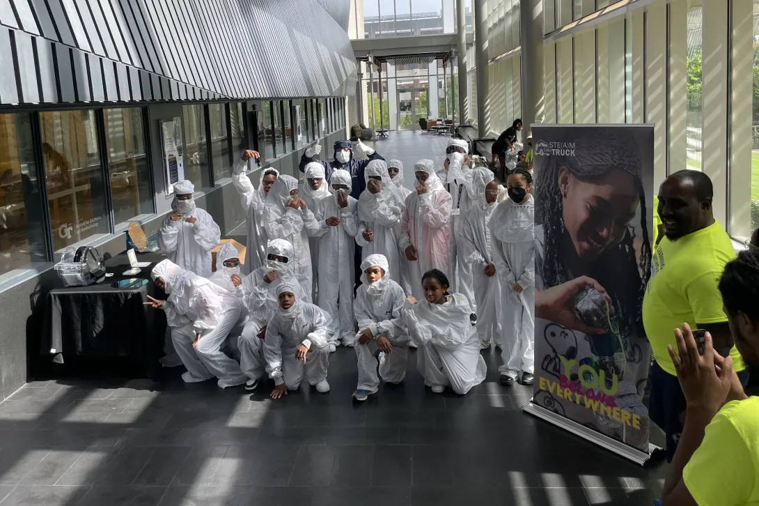
Sixth- through eighth-grade students sparked by this conversation can attend Chip Camp, a three-day STEM summer camp sponsored by Micron. They begin with a day at IEN to learn about thin films, magic sands, ferrofluids, and measuring their height in nanometers. The rest of the camp features hands-on visits to the Materials Characterization Facility (MCF) and the IEN cleanroom, where they can try on the white “bunny suits” technicians wear in the lab.
To further their reach, IEN’s workforce development team collaborates with teachers to bring nanotechnology into classrooms. During the summer, IEN offers the Research Experience for Teachers, a training program for public school and community college teachers to conduct nanotechnology research and learn how to incorporate it into their lessons. Middle school teachers have similar opportunities through the Nanoscience Summer Institute for Middle School Teachers.
Training the Workforce
When these students get to a university like Georgia Tech, IEN hires them for work-study jobs like the one Bonecutter-Leonard had. The hands-on cleanroom training is also vital to graduate students pursuing advanced degrees.
Katie Young earned her Ph.D. in materials science and engineering at Georgia Tech. Learning her way around the IEN cleanroom was essential for her graduate studies.
“My dissertation research involved synthesizing two-dimensional materials — only a single atom thick — for permeation barriers,” she explained. “I often used the cleanroom’s vacuum systems to synthesize and process 2D materials.” Now a research scientist at the Georgia Tech Research Institute, Young still works in the cleanroom on semiconductor device fabrication, building prototype quantum and biological sensors.
IEN opportunities are not limited to graduate research. Annually, about 150 Georgia Tech undergraduate students take microelectronics packaging and devices classes, with labs taught by IEN staff in the teaching cleanroom. These courses include Integrated Circuit Fabrication (ECE 4452), in which students learn to fabricate circuit elements, and the Science and Engineering of Microelectronic Fabrication (ChBE 4050/6050, open to graduate students as well), for students interested in semiconductor materials and fabrication.
Students don’t need to enroll at Georgia Tech to benefit from training, courses, and other opportunities. IEN’s internship program provides technical college students with training to become microelectronics technicians, either through work in the Biocleanroom or in the MCF.
Empowering Future Innovators
IEN also participates in the National Science Foundation Research Experiences for Undergraduates (REU), which provides opportunities for students from underrepresented groups or who attend schools without similar facilities. While enrolled at another university, John Mark Page was introduced to Georgia Tech’s cleanroom through an REU.
“That was my first exposure to any facility of this kind, and it felt like I was looking at the future. Being in a facility that can fabricate devices at or near the atomic level — it was hard to fathom,” Page said. “I had never thought that participating in microelectronics and nanotechnology as a student, especially as an undergraduate, was something I could do.”
As a result of his REU, Page transferred to Georgia Tech — he will graduate this summer with a bachelor’s degree in electrical engineering. He also completed a second REU at the University of North Carolina at Chapel Hill, worked as a student assistant in the IEN cleanroom, and participated in a Vertically Integrated Project (VIP), Chip Scale Power and Energy.
“I was interested in the VIP because it allowed me to spend more time in the cleanroom, familiarizing myself with semiconductor fabrication methods and training on new fabrication equipment,” Page explained. His experiences inspired him to consider a future career in the semiconductor industry.
“It wasn’t only the 10-week experience of the REU that made a lasting impact on me,” he said. “It was also the relationships formed with the people of IEN. The staff there are exceptional representatives of Georgia Tech, and they make IEN a tremendous asset to the future of microelectronics and nanotechnology in the U.S.”
Biya Haile, an ECE Ph.D. student, had a similarly meaningful REU experience. Haile, whose research focuses on creating micro-electro-mechanical systems-based sensors (MEMS), described the REU as “immersive.”
“The REU project enabled me to study chemical micro-sensor technologies, as well as state-of-the-art additive nano-manufacturing techniques, which has contributed to my research,” he said. “I feel lucky that my academic journey has entailed developing new technologies that use nanoscience to solve big problems.”
While Haile is currently focused more on designing and testing rapid processes for fabricating MEMS-based devices, he still occasionally works in the cleanroom on fabrication. He plans to go into the microelectronics industry after graduating.
The Path Ahead
All of IEN’s training and educational offerings align with IEN’s mission to bolster and diversify the microelectronics workforce, according to George White, senior director of strategic partnerships for the Georgia Tech research enterprise. “IEN has been at the forefront of the CHIPS infrastructure buildout, particularly in the area of education and workforce development,” he noted.
IEN’s efforts impact not just Atlanta but the entire country. Georgia Tech’s leadership in microelectronics research trains the innovators and practitioners of the future everywhere and ensures that America stays at the forefront of leading-edge technology. As demand increases for microelectronics, IEN is moving to meet it.
Effective July 1, 2024, the Institute for Electronics and Nanotechnology and the Institute for Materials will evolve into the Institute for Matter and Systems (IMS). This strategic union aims to foster convergent research at Georgia Tech, focusing on the science, technology, and societal underpinnings of cutting-edge materials and devices. Eric Vogel will be the director of IMS, and Michael Filler will be the deputy director.
Apr. 22, 2024

Effective July 1, Eric Vogel will become the executive director of the Institute for Matter and Systems (IMS), Georgia Tech’s newest Interdisciplinary Research Institute (IRI) that will launch on the same date.
As an evolution of the Institute for Materials (IMat) and the Institute for Electronics and Nanotechnology (IEN), IMS aims to enable convergent research at Georgia Tech related to the science, technology, and societal underpinnings of innovative materials and devices. Additionally, IMS seeks to integrate these innovations into systems that enhance human well-being and performance across information and communication, the built environment, and human-centric technologies that improve human health, wellness, and performance.
“Executive Vice President for Research Chaouki Abdallah and I are very excited about the launch of IMS, which positions Georgia Tech for integration of science and technology from atoms to devices, while explicitly drawing in researchers in the social sciences, design, business, and computing,” said Vice President of Interdisciplinary Research Julia Kubanek.
“IMS will ensure relevance across Georgia Tech through its newly configured Internal Advisor and Ambassador Board with representation across all six Colleges and GTRI,” she said. “Additional advisory committees representing IMS employees and facility users will ensure that we don’t sacrifice any of the research excellence for which IEN and IMat are known. With IMS I expect we will be even better positioned to tackle research problems that will have the greatest positive societal impact.”
Vogel will continue in his current position as the executive director of IMat until the launch of IMS. In addition to leading and growing IMat, Vogel is the Hightower Professor of Materials Science and Engineering at Georgia Tech’s School of Materials Science and Engineering, and he served as the IEN deputy director prior to leading IMat.
“It is an honor to be appointed executive director of the Institute for Matter and Systems, and I look forward to collaborating with the talented faculty and staff associated with it,” said Vogel. “This opportunity allows us to leverage the core competencies of IEN and IMat while extending our capabilities beyond nanotechnology and materials science. Together, we will be a hub for interdisciplinary research ranging from advanced materials to complex systems that solve global challenges.”
Georgia Tech’s IRIs facilitate collaboration between researchers and students from its six Colleges, the Georgia Tech Research Institute, national laboratories, and corporate entities to tackle critical topics of strategic significance for the Institute as well as for local, state, national, and international communities. IMS will also house and maintain the state-of-the-art Materials Characterization Facility and one of the largest academic cleanrooms in the nation, which offers a broad range of fabrication capabilities from basic discovery to prototype realization.
Before joining Georgia Tech in 2011, Vogel was an associate professor of materials science and engineering and electrical engineering at the University of Texas at Dallas. During this time, he also served as the associate director of the Texas Analog Center of Excellence and led UT Dallas’s involvement in the Southwest Academy for Nanoelectronics.
Prior to UT Dallas, he led the CMOS and Novel Devices Group and established the Nanofabrication Facility at the National Institute of Standards and Technology. Vogel holds a Ph.D. in electrical engineering from North Carolina State University and a B.S. in electrical engineering from the Pennsylvania State University. His research focuses on the development and fundamental understanding of electronic and nanomaterials and devices.
News Contact
Laurie Haigh
Research Communications
Apr. 16, 2024
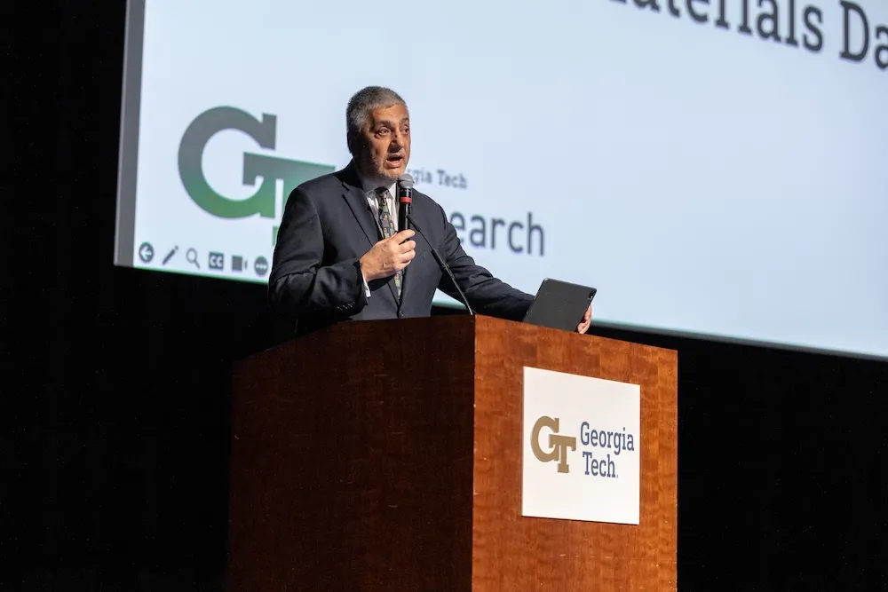
More than 400 people participated in Energy Materials Day on March 27, as researchers and industry leaders came together to discuss and advance energy materials technologies such as solar energy, carbon-neutral fuels, and batteries.
Energy materials are the things — natural, manufactured, or both — that aid the use of energy. They also play a key role in developing cleaner, more efficient energy solutions.
Energy Materials Day was co-hosted by Georgia Tech’s Strategic Energy Institute (SEI), the Institute for Materials (IMat), and the Georgia Tech Advanced Battery Center. The event evolved out of last year’s Georgia Tech Battery Day.
“As an engine of innovation in science and technology, Georgia Tech has incredible opportunities and the responsibility to conduct research to benefit society,” said Chaouki Abdallah, executive vice president for Research at Georgia Tech. “We call this ‘research that matters.’”
Events like Energy Materials Day are part of an ongoing, long-range effort to position Georgia Tech, and Georgia, as a go-to location for modern energy companies. Tech was recently ranked by U.S. News & World Report as the top public university for energy research. Abdallah also outlined why Georgia Tech, with more than 1,000 researchers across campus working in the energy space, is a natural fit for events that foster collaboration between the public and private sectors.
“Right here, right now, we have the opportunity to harness our collective powers, our collective knowledge, our collective resources to become a global engine of innovation,” he said.
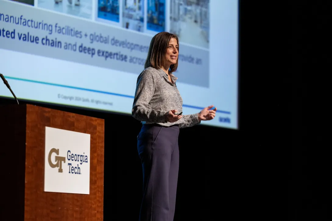
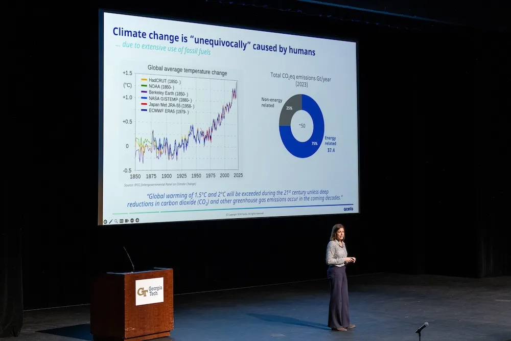
Plenary speaker Danielle Merfeld, global chief technology officer at QCells, highlighted opportunities for the current and future clean energy infrastructure in the United States.
"At the heart of our discussions today [are these questions]: What is new technology, and how do you make it ... and make it at scale, in an affordable, accessible, and reliable way?” she said.
"... [The] good news is this country has taken a very deliberate step toward creating the most robust industrial policy we've had in decades. ... This is driving opportunity and creating the foundation for manufacturing. So, [we can] use that industrial base of making and consuming power [and] decarbonize the electric grid by 2035...."
“Events like this are so important to forwarding progress in research and industry,” said Eric Vogel, IMat’s executive director. “It’s important to bring together professionals throughout the industry to keep these lines of communication open.”
The day was divided into three tracks: battery materials and technologies, photovoltaics and the grid, and materials for carbon-neutral fuel production. Attendees were encouraged to listen to talks from all three areas. Each track included academic speakers who shared their research and private-sector speakers who described how technological advancements are affecting the industry.
“With its rich history in energy research, Georgia Tech remains a leader in addressing global energy challenges,” said Tim Lieuwen, executive director of SEI. “The success of Energy Materials Day is encouraging, and I eagerly anticipate continuing these discussions in 2025.”
News Contact
Amelia Neumeister
Research Communications Program Manager
Mar. 26, 2024
Jud Ready, a principal research engineer at the Georgia Tech Research Institute (GTRI), has been selected to join the National Academy of Inventors’ (NAI) 2024 Class of Senior Members – a group of 124 academic inventors from NAI’s Member Institutions who have made significant contributions to innovation and technology.
Holding a dual appointment as Deputy Director of Innovation Initiatives for Georgia Tech’s Institute for Materials, one of Tech’s 10 Interdisciplinary Research Institutes (IRI) focused on advancing materials research and innovation, and with over two decades of experience as an adjunct professor in Tech’s School of Materials Science & Engineering, Ready has established himself as a leader in materials science and engineering.
Read the full story
News Contact
Michelle Gowdy
(Interim) Director of Communications, GTRi
Mar. 13, 2024
Muhannad Bakir has been named director of the Institute for Electronics and Nanotechnology’s 3D Systems Packaging Research Center (PRC).
"We’re thrilled to have Professor Bakir joining us as the new director,” said Michael Filler, IEN’s interim executive director. “His wealth of experience and pioneering work in advanced packaging make him an excellent fit to lead the PRC into an exciting new era of innovation and technological impact.”
Originating as a National Science Foundation Engineering Research Center in 1993, the PRC is a national leader in the advanced packaging of microelectronics. Advanced packaging in microelectronics refers to innovative techniques for merging and interconnecting multiple components within a single electronic entity. This enables more powerful, efficient, and versatile microelectronic systems, driving innovation across various industries. The Center conducts research and education in all aspects of electronics packaging, including design, materials, process, assembly, thermal management, and system integration. Its work is driven by a wide range of applications, such as high-performance computing, artificial intelligence, automotive systems, wireless communications, and space exploration.
“I am honored for the opportunity to lead the PRC and look forward to working with the campus community and our industry, government, and academic partners on a research agenda that tackles the multifaceted challenges in advanced packaging and heterogeneous integration,” said Bakir.
As director, Bakir will guide the PRC into the future of advanced packaging through his vision and expertise. He is responsible for ensuring that the PRC's world-class facilities support the emerging needs of advanced packaging of microelectronics and supports members of the campus community who uses these facilities.
“We are excited to lead the science and engineering that culminates in system level prototyping and demonstrators for AI, mm-wave, photonic systems, and beyond,” he said.
Bakir, who also serves as the Dan Fielder Professor in the School of Electrical and Computer Engineering and leads the Integrated 3D Systems Group, brings a wealth of experience to his new role as PRC director. He and his research group have received more than 30 paper and presentation awards including seven from the IEEE Electronic Components and Technology Conference, four from the IEEE International Interconnect Technology Conference, and one from the IEEE Custom Integrated Circuits Conference. His group was also awarded the 2014 and 2017 Best Papers of the IEEE Transactions on Components Packaging and Manufacturing Technology.
Bakir is the recipient of the 2013 Intel Early Career Faculty Honor Award, 2012 DARPA Young Faculty Award, 2011 IEEE CPMT Society Outstanding Young Engineer Award, and was an Invited Participant in the 2012 National Academy of Engineering Frontiers of Engineering Symposium. He is the co-recipient of the 2018 IEEE Electronics Packaging Society Exceptional Technical Achievement Award “for contributions to 2.5D and 3D IC heterogeneous integration, with a focus on interconnect technologies.” He is also the co-recipient of the 2018 McKnight Foundation Technological Innovations in Neuroscience Awards. In 2020, Bakir received the Georgia Tech Outstanding Doctoral Thesis Advisor Award.
He serves as a senior area editor for the IEEE Transactions on Components, Packaging and Manufacturing Technology and was previously an Editor for IEEE Transactions on Electron Devices. He has also served as a distinguished lecturer for IEEE EPS.
News Contact
Amelia Neumeister
Research Communications Program Manager
Mar. 04, 2024
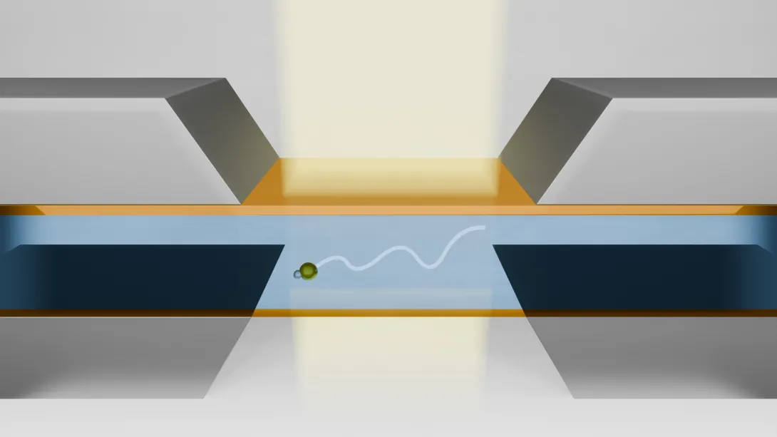
The Institute for Electronics and Nanotechnology (IEN) at Georgia Tech has announced the 2023 IEN Exponential Electronics (IEN-EX) Seed Grant winner, Vida Jamali, Assistant Professor in the School of Chemical and Biomolecular Engineering at Georgia tech.
The primary purpose of this program is to give early-stage research and development to create revolutionary electronic systems.
IEN-EX provides seed funding for Georgia Tech researchers to pursue “1000x” ideas within electronics or that bridge electronics with other technical domains. “1000x” ideas are those with the potential to improve one or more well-defined, but often overlooked or underappreciated performance metrics by at least 1000x.
In this brief Q&A, Jamali discusses her research focus, how it relates to electronics research, and the impact of this initiative.
- What is your field of expertise and at what point in your life did you first become interested in this area? In situ liquid phase transmission electron microscopy. I started learning about this tool when I was a postdoc to develop it as a single particle tracking method.
- Briefly explain your research: My research is focused on investigating the dynamics of nanoscale objects in their native liquid environment, from synthetic colloidal nanomachines to biological macromolecules, using liquid phase transmission electron microscopy. We develop experimental and computational tools to visualize and characterize dynamic behavior (equilibrium and non-equilibrium) at small length scales and in real-time.
- Who are the PIs: Me and Amirali Aghazadeh, Assistant Professor in the School of Electrical and Computer Engineering.
- What questions or challenges sparked your current research? Is it possible to use an electron microscope and capture the dynamics of nanoscale materials in time as they move and interact with each other and respond to their surrounding environment with a high spatiotemporal resolution?
- How is your research working to create revolutionary electronic systems? We design and develop a new nanoelectronic coded aperture device that once integrated into transmission electron microscopes can increase resolution exponentially.
- What are the broader global and social benefits of the research you and your team conduct? Once realized this technology opens a new window into dynamic phenomena at a scale inaccessible before. This unprecedented level of information will significantly advance areas from drug discovery impacting human health to achieving single crystalline materials for the semiconductor industry.
- How will this funding support your research? This funding will support graduate students who will be realizing this idea
News Contact
Amelia Neumeister
Research Communications Program Manager