May. 19, 2026
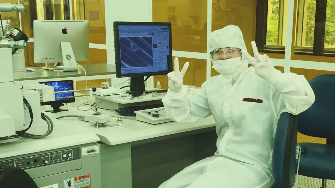
Home to the largest academic cleanroom in the Southeast, the Institute for Matter and Systems (IMS) prides itself on its outstanding employees. From laboratory operations to education and outreach, these employees are central to IMS’s continued success.
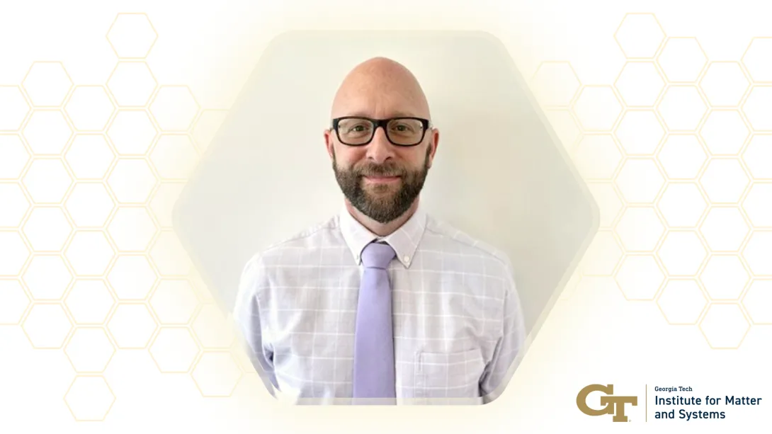
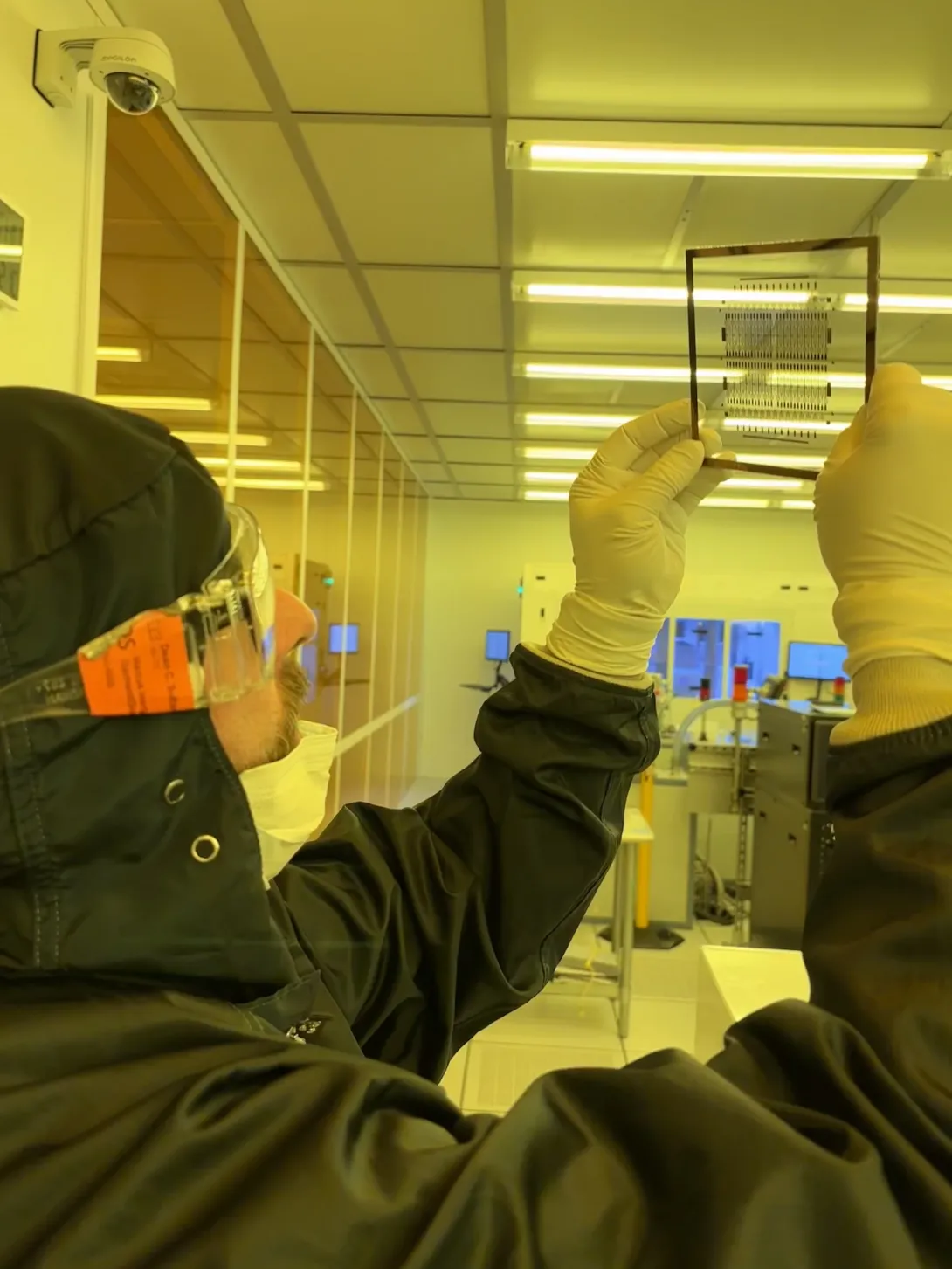
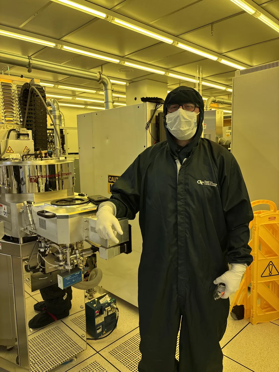
One employee in particular, Dean Sutter, has supported the success of IMS for more than 18 years. As process equipment engineering manager, Sutter leads a team of engineers responsible for optimizing and maintaining equipment and manufacturing processes in the cleanroom.
In the following Q&A, Sutter discusses some of his favorite moments, challenges, and surprises during his time at IMS.
What is your favorite aspect of your job?
"Every day presents new challenges. It is never the same thing from day to day"
What has been your most rewarding challenge?
“Getting the PlasmaTherm Single Chamber running after multiple months of downtime.”
What is your favorite project you are working on or have worked on?
"Modifying lab equipment to enable our users to get the results they are after."
Since February, what equipment have you modified and how?
“We haven't had to modify anything lately, but we started bringing some of our more than 30-year-old tooling up to modern equipment standards in terms of vacuum components and control systems. An example would be going from bearing turbo pumps to magnetically levitated pumps and Windows 95 to modern programmable logic controllers.”
What has been your favorite lab equipment to work with?
“I do not have any favorites, but I do like seeing all the presentations from our users on the research being done in the cleanroom. I also enjoy attending Ph.D. defense presentations and seeing the completed work.”
What is something you never thought you would learn in this position?
“Learning the personal side of employee management. As an equipment engineer–not a manager–there is a pretty distinct separation between the personal and professional sides of people. In management, those lines are blurred, and you have to deal with both.”
You have been with IMS for 18 years. What has kept you here all these years?
“This organization has allowed me to substantially grow my professional career over the years. I started with Bob Rose and then transitioned to Gary Spinner's team. Both gentlemen have been great mentors!”
Do you have any hobbies outside of work? Tell us about them.
“I am an auto mechanic outside of Tech. I have rebuilt engines, worked on automatic transmissions, and done electrical troubleshooting. I enjoy building cars from the late 1920s, similar to the Ramblin’ Wreck, through the late 1960s. My current project is a 1949 Ford Truck. I also do construction, plumbing, electrical, mechanical, and heavy equipment operation, such as running excavators. I’m always up for learning a new skill.”
News Contact
Writer: Gabriel Buggi | Communications Student Assistant
Media Contact: Amelia Neumeister | Communications Manager
The Institute for Matter and Systems
May. 18, 2026

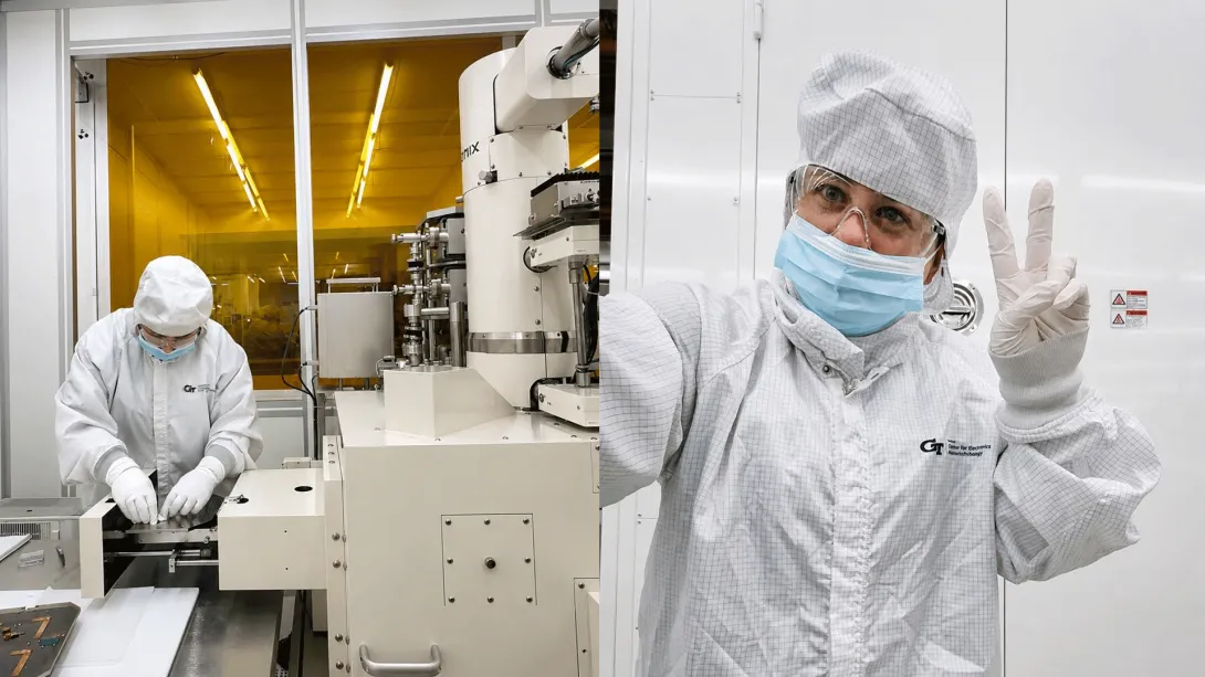
Asif Khan and Lance Fernandes built the ferroelectric NAND memory chips in Georgia Tech’s cleanroom, then sent the chips for radiation testing to collaborators at Pennsylvania State University. Those tests revealed just how extreme the technology’s tolerance could be.

Lance Fernandes and Asif Khan in the cleanroom.
As space missions travel farther from Earth, spacecraft must increasingly be able to process and store their own data. Soon, artificial intelligence (AI) could be the primary tool for handling this growing volume of information. NAND flash memory is the current state-of-the-art technology used to store these massive amounts of data, offering storage capacities in the terabit range. It’s the same technology used in laptops, smartphones, and data centers. Ensuring NAND’s reliability in space is critical as these systems increasingly rely on high-density, low-power storage.
But the radiation in harsh space environments can significantly degrade data stored in NAND flash memory. To counteract this, Georgia Tech researchers have developed a new form of NAND flash memory that can both handle AI and withstand extreme radiation.
This technology uses ferroelectricity, which is when certain materials can hold a permanent, spontaneous electric charge, called polarization. In a recent Nano Letters paper, the researchers show that NAND flash memory made with ferroelectric materials can withstand radiation levels up to 30 times higher than more conventional NAND flash memory.
“If you send traditional flash memory to space, the radiation interacting with flash memory’s trapped electric charge can easily corrupt the data,” said Asif Khan, an associate professor in the School of Electrical and Computer Engineering (ECE). “In contrast, ferroelectric NAND flash storage does not store data as trapped electrical charge, but rather stores it as polarization in the material. And polarization is very resilient to radiation effects.”
Radiation Revelation
The insight that NAND flash-compatible ferroelectric memory could withstand high amounts of radiation surprised the researchers. Ferroelectricity in hafnium oxide — the silicon-compatible material that makes this memory possible — was discovered just 15 years ago, and Khan’s lab has been determining its capabilities for the past decade. The team knew ferroelectricity was radiation-tolerant, but not exactly how tolerant when implemented in NAND flash architectures.
Lance Fernandes, an ECE Ph.D. student and the paper’s first author, built the ferroelectric NAND memory chips in Georgia Tech’s cleanroom, then sent the chips for radiation testing to collaborators at Pennsylvania State University. Those tests revealed just how extreme the technology’s tolerance could be.
The Penn State researchers’ testing showed that ferroelectric flash technology can sustain radiation as high as 1 million rads (radiation absorbed doses) — the equivalent of 100 million X-rays — making it 30 times more durable than traditional memory. This is well within the radiation-tolerance threshold for most spacecraft: Low-Earth orbit satellites require a tolerance of 5 – 30 kilorads, geostationary orbits need 100 – 300 kilorads, and deep space missions top out at 1 million rads.
“For data storage in space, it’s not enough for memory to work. It has to remain reliable under extreme radiation,” said Fernandes.
“And what makes our storage especially exciting," added Khan, “is that ferroelectric NAND flash isn't just radiation-tolerant; it also stays reliable even in extremely harsh radiation environments. That's exactly what we need for space.”
From orbiting satellites to future missions surveying Jupiter’s moons, successful space exploration requires electronics that can process abundant AI data and will not fail when communication is delayed. Ferroelectric memory offers a way to keep critical data intact, no matter how harsh the environment.
The work was supported in part by SUPREME, one of seven centers in JUMP 2.0, a Semiconductor Research Corporation (SRC) program sponsored by DARPA. The work was performed as part of the Interaction of Ionizing Radiation With Matter University Research Alliance, sponsored by the Department of Defense, Defense Threat Reduction Agency, under grant HDTRA1-20-2-0002.
Enabling Radiation Hardness in Solid-State NAND Storage Utilizing a Laminated Ferroelectric Stack Lance Fernandes, Stuart Wodzro, Prasanna Venkatesan, Priyankka Ravikumar, Ming-Yen Lee, Minji Shon, Dyutimoy Chakraborty, Taeyoung Song, Sanghyun Kang, Salma Soliman, Mengkun Tian, Jason Yeager, Jackson Adler, Jiayi Chen, Zekai Wang, Douglas Wolfe, Shimeng Yu, Andrea Padovani, Suman Datta, Biswajit Ray, and Asif Khan. Nano Letters 2026 26 (10), 3390-3397
DOI: 10.1021/acs.nanolett.5c05947
News Contact
Tess Malone, Senior Research Writer/Editor
tess.malone@gatech.edu
May. 18, 2026

A photo of Vida Jamali, assistant professor the School of Chemical and Biomolecular Engineering; Amirali Aghazadeh, assistant professor in the School of Electrical and Computer Engineering; and Josh Kacher, associate professor in the School of Materials Science and Engineering standing in front of a TEM at Georgia Tech.
Scientific discovery is often portrayed as the result of long hours alone in a lab, but true science is inherently collaborative. The most robust experimental processes are developed through partnerships across multiple areas of research. The need for specialized, multidisciplinary teams slows experiment design, execution, data analysis, and process updates, delaying technological validation and deployment. But if the increasingly automated tools scientists already use in the lab could contribute to this team process of experimental design, the timeline for these goals could be greatly accelerated.
This concept of “lab tool as lab assistant” is the premise of a recent paper in npj | Computational Materials titled “Thinking Microscopes: Agentic AI and the Future of Electron Microscopy,” by Vida Jamali, assistant professor the School of Chemical and Biomolecular Engineering; Amirali Aghazadeh, assistant professor in the School of Electrical and Computer Engineering; and Josh Kacher, associate professor in the School of Materials Science and Engineering.
In the paper, the team introduces the concept of “thinking electron microscopes,” in which agentic AI systems are directly integrated with the instrument. This allows microscopes to move beyond their conventional role as characterization tools and toward functioning as co-scientists for human users.
Drawing on advances in specialized large language models, or LLMs, that demonstrate their ability to collaborate, reason over data, and integrate prior knowledge, the team envisions specialized LLM-based agents assigned to specific roles and areas of knowledge expertise. By explicitly incorporating domain knowledge into specialized agents and distributing information across multiple agents with focused expertise, the approach enables parallel evaluation of competing hypotheses, clearer separation of roles — such as planning, simulation, and critique — and more transparent and robust reasoning.
Within the experimental pipeline, these agents can analyze materials’ properties, physical data, chemical processes, and other relevant parameters. They could also collaborate with an agent that specializes in experimental design, refining iterative closed-loop experimentation, and real-time scientific discovery.
Although the research focuses on AI collaboration, the team notes that human researchers must retain accountability for the accuracy and integrity of both the experimental process and the results reported. This oversight begins with advocating for greater open access to research materials in all formats, building community-driven data repositories, and adopting standardization in how experimental parameters and metadata are reported. Equally important, researchers should be willing to report data from failed experiments as well as successful outcomes. Finally, organizations should work together to standardize secure APIs that enable shared, remote access to infrastructure across distances.
We see this as a step toward scientific instruments that do more than acquire data; systems that can reason over experiments, adapt measurements, and participate in the scientific discovery process alongside researchers. - Vida Jamali, assistant professor the School of Chemical and Biomolecular Engineering
The team is already developing these systems by connecting cloud-based, agentic infrastructures to microscopes at the Institute for Matter and Systems at Georgia Tech. With the addition of agentic AI, the goal is to accelerate discovery and engineering of new nanoscale materials for energy and quantum applications, as well as advance capabilities in cryo-electron microscopy and structural biology. These tools can optimize data collection, link real-time microscope observations with structural models of proteins, and dynamically adjust and prioritize experiments. The team sees this work as the first step toward the next generation of “thinking” electron microscopes, as well as an advancement in scientific discovery across domains.
- Christa M. Ernst
This research is supported by the Institute for Data Engineering and Science and the Institute for Matter and Systems
Original Publication
Jamali, V., Aghazadeh, A. & Kacher, J. Thinking microscopes: agentic AI and the future of electron microscopy. npj Computational Materials 12, 149 (2026). https://doi.org/10.1038/s41524-026-02077-y
News Contact
May. 15, 2026
The University System of Georgia Board of Regents (BOR) honored 19 Georgia Tech faculty and researchers across campus with Regents’ appointments at its April meeting.
Among those recognized is Yong Ding, principal research engineer and electron microscopy core lead at the Materials Characterization Facility (MCF) within the Institute for Matter and Systems (IMS), who was named a Regents’ Researcher.
Ding received his Ph.D. in Physics from Nanjing University. Since joining Georgia Tech in 2003, he has made widespread contributions to interdisciplinary materials research through collaborations with faculty, national laboratories, and industry partners, enabling advanced materials characterization and scientific discovery. His current work focuses on the development and application of advanced transmission electron microscopy (TEM) techniques, including in-situ TEM, electron tomography, and quantitative spectroscopic analysis. He also leads major instrumentation initiatives, including the acquisition and deployment of the Thermo Fisher Scientific Spectra Ultra TEM.
Ding’s work has had a significant impact on nanoscience, catalysis, and energy materials. In addition to his research, he is a dedicated educator and mentor, providing training to dozens of microscopy users annually and teaching courses in electron microscopy and nanomaterials.
The Regents’ Awards are among the University System of Georgia’s highest honors, recognizing sustained excellence, national distinction, and long-term impact by faculty and researchers across the state’s public institutions.
Regents’ distinctions may be granted to outstanding faculty members for a period of three years by the BOR and are awarded only after unanimous recommendation from the president of the recipient’s university, their chief academic officer and dean, and three additional members of the faculty who are named by the university president. Approval by the chancellor and the BOR Committee on Academic Affairs is also required. These distinctions are given to those who make outstanding contributions to their respective institutions.
May. 11, 2026
In the summer of 2019, Caroline Howell came to Georgia Tech for the first time to participate in the NNCI Research Experience for Undergraduates (REU). As a student at Troy University in Alabama, Howell was looking to broaden her research horizons.
“I went to a smaller university because I came from a very, very small town,” she said. “I did some research there, but we didn’t have a lot of equipment or resources.”
During the 10-week program, undergraduate students live on campus and conduct research in faculty labs with mentorship and access to advanced facilities. The program also prepares students for graduate studies and STEM careers through professional development, research communication training, and opportunities to present their work.
“I applied to the REU at Georgia Tech. And when I got in, I was super excited because Georgia Tech is a big deal,” she said.
That summer didn’t just expand her lab experience; it reshaped her career trajectory.
As a physics major, Howell had never been exposed to materials science, nanotechnology, or cleanroom environments before arriving in Atlanta. That summer marked her first time using advanced equipment, including scanning electron microscopes (SEMs), and working hands-on in Georgia Tech’s cleanroom facilities.
Her project focused on aluminum alloys, testing their strength and fracture behavior under simulated harsh conditions such as saltwater and heat. The research explored how lightweight, affordable materials like aluminum could be made stronger for applications such as shipbuilding.
The experience opened a door for Howell.
“It inspired me to go to grad school for materials science,” she said.
After completing her undergraduate degree at Troy University, Howell pursued graduate studies in materials science at the University of Colorado Boulder, where she earned her master’s degree.
Her REU experience gave her a technical advantage early in her career.
“In my first job, I worked with the same machines I used at Tech because I already had experience with them,” she said.
Today, Howell is back at Georgia Tech. This time not as a student, but as an industry researcher using the Institute’s cleanroom facilities as part of her full-time job.
She conducts advanced lithography and SEM analysis in the same facilities, expanding far beyond what she was able to do as an undergraduate. Still, she credits the REU with giving her a strong foundation.
“I came in already knowing how to do some things, and it’s just kind of cool to be back in the same space I was in years ago,” Howell said.
In a full-circle moment, the place that first introduced her to materials science is now part of her professional experience.
For Howell, the impact of the REU extended well beyond lab work. The REU provided her technical training, exposure to a new discipline, and the confidence to pursue graduate education. It connected her with mentors who supported her next steps and introduced her to equipment she would later use professionally.
For students considering an REU, her advice is simple:
“Do it.”
Sometimes, a single summer can shape an entire career — and even bring you right back to where it all began.
May. 06, 2026
: Mustafa Ali, Armond Duncan, and Roshan Padhan</p>")
The 2026 HBCU CHIPS Network Conference, co-hosted by Georgia Tech and held April 1-2 at the Renaissance Atlanta Midtown Hotel, brought together students, faculty, researchers, industry leaders, and federal partners to advance innovation and workforce development in the U.S. semiconductor ecosystem. By pairing technical programming with a dedicated career fair, the event emphasized both learning and direct access to opportunities.
Now in its second year, the conference continues to grow as a national platform for collaboration across more than 30 Historically Black Colleges and Universities (HBCUs), all working to strengthen diversity and talent pipelines in microelectronics and semiconductor industries. Centered on the theme of Championing New Approaches to Reestablishing U.S. Dominance in Semiconductors and Microelectronics, the event featured technical sessions, panel discussions, poster presentations, and networking opportunities.
“This conference provides a national platform to showcase the depth of talent within the HBCU community, including leading edge research and innovation,” said George White, executive director of strategic partnerships and chief CHIPS strategy officer at Georgia Tech. “It also raises awareness of public and private funding opportunities and promotes collaboration across academia, industry, and government.”
Attendance reflected strong interest across the network. The conference drew approximately 180 participants, including representatives from 26 HBCUs, 17 industry and nonprofit organizations, five government agencies, and the Technical College System of Georgia. The career fair attracted 231 students from the same 26 institutions.
The addition of the career fair this year, which created space for more focused interaction between students and employers, gave students opportunities to speak one-on-one with recruiters and industry professionals. These conversations gave them a clearer understanding of career pathways, available roles, and how to enter the field.
“This experience strengthened my interest in pursuing a career in the semiconductor industry, particularly in fabrication, validation, and reliability,” said Mustafa Ali, a student at Prairie View A&M University and a Student Achievement in Microelectronics Award recipient. “Engaging with both industry professionals and the academic community showed me the importance of connecting research with real-world applications.”
The addition of the career fair also reflects the broader mission of the HBCU CHIPS Network: not only to advance research, but also to build a robust, diverse talent pipeline ready to meet the nation’s growing demand for semiconductor professionals. With the U.S. projected to need tens of thousands of new workers in this sector in the coming years, integrating a career fair directly into the conference experience ensures that students are not just participants in conversations, but active candidates in the future workforce.
Six employers participated in the career fair: Savannah River National Laboratory, Sandia National Laboratories, Teradyne, GlobalFoundries, Synopsys, and Micron. They offered internships and full-time positions, while also connecting with students interested in long-term career development. Graduate programs from Clark Atlanta University, Norfolk State University, Georgia Tech, and North Carolina A&T State University were also represented, highlighting academic pathways alongside industry roles.
“At Teradyne, we believe that innovation thrives when our teams reflect the full spectrum of talent and perspectives that exist across the engineering landscape,” said Danielle S. Ferguson-Macklin, talent communities program manager at Teradyne. “HBCUs have a proven legacy of cultivating exceptional STEM talent, and partnering with these institutions allows us to connect with students who bring both technical rigor and a deep sense of purpose to their work. Strengthening our HBCU recruiting pipeline is not a diversity initiative; it is a strategic investment in the future of our workforce and the semiconductor industry.”
“We look for students with strong technical foundations, intellectual curiosity, and the adaptability to thrive in fast-moving, complex environments,” added Armond Duncan, staff program manager, MSI network collaboration, at Micron. “Collaboration, communication, and a willingness to continuously learn are just as critical as technical acumen. Students who demonstrate hands-on experience and a clear sense of purpose are best positioned to make an immediate and lasting impact.”
Beyond recruitment, the event placed a strong emphasis on mentorship and networking. Many students sought guidance in addition to job opportunities, and the format of the career fair, supported by shared meals and informal spaces, encouraged natural conversations and relationship-building. For some students, the experience highlighted the value of connecting research to industry trends.
“Attending the conference was an extremely enriching experience,” said Roshan Padhan, a student at Jackson State University and another Student Achievement in Microelectronics Award recipient. “It further motivated me toward the advancement of next-generation semiconductor devices and provided a broader understanding of how academic research translates into real-world technological innovations.”
Sustained engagement throughout the event highlighted the demand for career-focused programming within the HBCU CHIPS Network. Organizers expect that demand to continue growing. “In the coming years, we expect the conference to expand in scope and impact,” White said. “Ultimately, our goal is for many — if not all — HBCUs to have awareness of, representation at, and meaningful participation in the conference.”
News Contact
May. 05, 2026
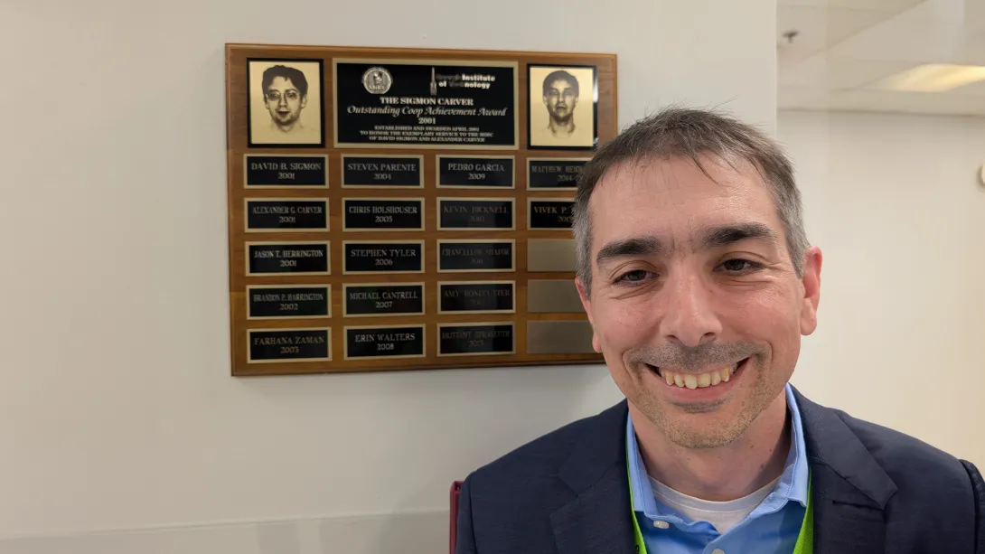
The most unassuming actions can have the greatest outcomes. For Brandon Harrington, CmpE 2005, M.S. CmpE 2008, walking through the doors of the Pettit Microelectronics Building, then home to the Microelectronics Research Center (MiRC), during his freshman year 25 years ago changed the course of his career.
Each week on his way to the Howey Physics Building, Harrington passed the MiRC, wondering what happened behind its doors.
“One day I got the courage to walk in. I went to the front desk and I asked, ‘Hey, do you have any jobs for freshmen?’” Harrington recalled. “I was pointed to Bob Rose, so I walked down and had a brief conversation with him where he hired me on the spot.”
That moment—walking in with curiosity and leaving with a job— shifted Harrington’s career path from pursuing a bachelor’s degree in computer engineering and working in electronic design automation (EDA) to a life in the laboratory advancing microelectronics research.
When he began working for the MiRC in the early 2000s, the cleanroom facilities had only three full-time employees. The small staff gave Harrington opportunities to contribute. He started with smaller tasks, from changing pump oil to sorting nuts and bolts, but his dedication quickly led to greater responsibility.
At the time, Gary Spinner, director of cleanroom operations for the Institute for Matter and Systems (IMS), played a key role in mentoring students and expanding access to the Institute’s microelectronics facilities. Known for his hands-on approach and commitment to student development, Spinner helped guide the growth of cleanroom operations and the people who worked within them.
“Gary took note of me and said, ‘Brandon, please join the co-op program,’” Harrington said. “I quickly found my way into the cleanrooms, and from that point on, I touched basically every system, whether it was the billing software, the access control system, or the toxic gas monitoring.”
As an undergraduate co-op, Harrington advanced through the MiRC, training graduate researchers on tools and developing new or modifying existing efficiency systems. By the time he earned his undergraduate degree, he had accumulated extensive experience in the cleanrooms and graduated with an offer to be a full-time electrical engineer for the MiRC while pursuing his master’s degree.
An unexpected outcome of this role was a friendship that led him to a Ph.D. in electrical engineering. While working full-time, Harrington became good friends with then-Ph.D. student Reza Abdolvand. After Abdolvand joined Oklahoma State University as a faculty member, he asked Harrington if he would come help him start his research group.
“I was really good friends with Reza and I thought this was a way I could get his career going,” Harrington said. “So I left Georgia Tech, around 2008, to pursue my PhD from Oklahoma State.”
Today, Harrington supports the industry in a variety of ways, providing consultation for startups and large corporations alike. His work includes early feasibility studies, prototype development, productization, transfer to volume-production foundries, and yield improvement activities.
He is now the director of microelectromechanical systems (MEMS) development at AMFitzgerald, where he leads a team delivering innovative solutions to clients—all because he followed his curiosity.
Harrington’s journey reflects the broader impact of Georgia Tech’s cleanroom facilities—spaces where curiosity can turn into hands-on experience, mentorship, and career-defining opportunities. By providing students access to advanced tools, real-world problem-solving, and a collaborative research environment, the cleanrooms continue to shape the next generation of engineers and innovators, just as they did for a curious freshman who decided to walk through an open door.
News Contact
Writer: Gabriel Buggi | Communications Student Assistant
Media Contact: Amelia Neumeister | Communications Manager
The Institute for Matter and Systems
Apr. 28, 2026

Chris Rozell is giving the opening remarks at the ATL Neuro Networking and Symposium Night.

A group of students is discussing a poster, and the presenter is giving an example during the first poster session.

A group of students and faculty is discussing a poster during the second poster session.

A group of students and faculty is discussing a capstone poster during the second poster session.
At Georgia Tech, undergraduate students are an integral part of the research enterprise – particularly when it comes to neuroscience. That dedication to undergraduate research was on full display on April 8, when more than 100 students from Atlanta-area universities gathered for the annual ATL Neuro Networking and Symposium Night.
This student-run event, hosted by the Georgia Tech Student Neuroscience Association (SNA) and co-sponsored by the Institute for Neuroscience, Neurotechnology, and Society (INNS) and the Neuroscience Undergraduate Program at Georgia Tech, aimed to bring together students and faculty from the broader Atlanta neuroscience community for an evening of data-blitz talks showcasing faculty research, undergraduate poster presentations, and catered networking.
“Our goal was to bridge the gap between Atlanta’s institutions and showcase the diversity of undergraduate research,” says Harshin Vijay, symposium director of SNA. “By bringing these groups together through SNA, we’re fostering an ecosystem where the next generation of scientists can exchange ideas and build collaborative networks essential for future innovation."
The impact of undergraduate neuroscience research is “more than bench to bedside,” said INNS Executive Director Chris Rozell at the event. “It’s about advancing neuroscience and neurotechnology to improve society through discovery and innovation. Undergraduate research catalyzes innovation – invigorating and advancing educational programs through collaboration that empowers society – fueling impact and fostering the community of next-generation scientists.”
Featuring more than 40 undergraduate posters, research topics ranged anywhere from the impact of music on associative memory to the role of taste projection neurons in Drosophila. Some students even examined their own coursework, either as a TA or their involvement with capstone research.
“There are neuroscientists in every College at Georgia Tech, and we have undergraduate neuroscience students performing research all over campus and in the broader Atlanta neuroscience community,” says Katharine McCann, the director of Undergraduate Research for Georgia Tech’s neuroscience program. “Events like this bring those students together to learn from each other and broaden their networks. It is exciting to see so many students passionate about their research.”
Four posters were awarded for their work:
Best Poster Design: “Role of Taste Projection Neurons in Drosophila Taste Processing”
- Hanti Jiang, Emory University
Best Presentation: “Neuroscience and Computer Science Roots of Pattern Recognition”
- Rishi Polepally, Georgia Tech
- Aryan Kumar, Georgia Tech
- Vedanth Natarajan, Georgia Tech
Best 4001 Group: “Evaluating Cognitive Engagement in AI-Generated VS. Human-Created Educational Content”
- Hannah Ammari, Georgia Tech
- Shobini Palaniappan, Georgia Tech
- Rayhan Quraishi, Georgia Tech
- Aryan Shah, Georgia Tech
- Divya Tadanki, Georgia Tech
People's Choice Award: “Vibration as an effective facilitation of sensorimotor learning in Blaptica dubia cockroaches”
- Diana Sethna, Georgia Tech
- Jacob Hayes, Georgia Tech
- Ellie Kate Watson, Georgia Tech
- Arya Oak, Georgia Tech
Esha Panse, Georgia Tech
- Hersh Mathur, Georgia Tech
News Contact
Writer: Hunter Ashcraft
Communications Student Assistant
Institute for Neuroscience, Neurotechnology, and Society
Media Contact: Audra Davidson
Research Communications Program Manager
Institute for Neuroscience, Neurotechnology, and Society
Apr. 24, 2026

Professor Emmanouil “Manos” Tentzeris and Ph.D. student Marvin Joshi hold a lens‑enabled backscatter system that could support battery‑free wireless communication across future smart city infrastructure.

Shown near existing campus emergency infrastructure, the lens‑enabled backscatter device highlights how ultra‑low‑power wireless systems could be integrated directly into everyday infrastructure without relying on batteries or wired power.

A close‑up view of the device displays an array of tiny antenna elements positioned behind the lens, each modulating reflected wireless signals to enable high‑speed communication with minimal energy use.

A concept illustration shows how the lens-enabled system’s wide angular coverage and passive backscatter communication enable flexible deployment on moving platforms such as drones and aircraft, as well as fixed smart city infrastructure and personal devices.
Earlier this year, Georgia Tech researchers showed that specially designed lenses could harvest energy from ambient wireless signals, pointing toward a future of battery-free sensors embedded throughout smart cities and digital infrastructure.
But powering devices is only part of the challenge. Enabling those same systems to communicate at modern data rates is a much harder. That’s the leap the team is now making. The same lens-based approach is being used to unlock high-speed communication once considered out of reach for ultra-low-power systems.
In a study published in Nature Communications, researchers in Professor Manos (Emmanouil) Tentzeris’ Agile Technologies for High-performance Electromagnetic Novel Applications (ATHENA) lab demonstrated a first-of-its-kind lens-enabled backscatter system capable of multi-gigabit data rates, reaching up to 4 gigabits per second (Gbps). At the same time, it operates using only a fraction of the power required by conventional wireless devices — bringing high-speed connectivity to systems that were never meant to support it.
For years, backscatter has been treated as a tradeoff: extremely low power, but extremely limited performance. Rather than generating its own radio signal, a backscatter device modulates and reflects existing wireless transmissions to communicate, allowing it to operate with minimal energy.
As a result, backscatter has typically been used only to send small amounts of data, most often in simple identification and sensing systems.
“What we’ve shown is that backscatter doesn’t have to be slow,” said Marvin Joshi, the research lead and Ph.D. candidate in the School of Electrical and Computer Engineering. “With the right architecture, it can operate at gigabit‑per‑second speeds while remaining ultra‑low power.”
The Lens That Makes It Possible
The Georgia Tech team’s dielectric lens — similar in spirit to an optical lens — focuses incoming millimeter-wave energy onto an array of tiny antenna elements, enabling both wireless energy capture and high‑speed backscatter communication within the same system.
The system reshapes and reflects existing wireless signals, with each element modulating the reflected signal to enable high-speed data transmission without requiring a traditional transmitter.
At millimeter-wave frequencies, used by 5G and future 6G systems, there is plenty of available bandwidth, but signals at these frequencies are highly directional and sensitive to alignment.
In practice, that means even small misalignment can break the link. This has been a major limitation for real-world deployment. The lens overcomes that constraint by enabling high gain and wide angular coverage simultaneously, without the need for active beam steering.
“Think of it like a camera lens for wireless signals,” Tentzeris said, who is a Ed and Pat Joy Chair Professor in ECE. “It captures energy coming from many different directions and focuses it efficiently onto the device.”
The result is a system that can communicate over a ±55-degree field of view, maintaining strong performance even when the device and the reader are not perfectly aligned.
Fiber-Level Speeds, Nearly Zero Power
In controlled experiments, the researchers achieved data rates of up to four Gbps, with sustained gigabit communication at distances of up to 20 meters, using high-order modulation schemes like those used in modern cellular networks.
For a system that doesn’t generate its own signal, those numbers are unexpectedly efficient. The system operates at just 0.08 picojoules per bit — approaching million-fold improvements compared to conventional wireless radios.
“To put that in perspective,” Tentzeris said, “a typical wireless transmitter burns milliwatts of power. This system operates at essentially near-zero power while pushing the data rates 1,000 times higher than what traditional backscatter could do.”
Taken together, the results point to a fundamentally different class of wireless system, according to Tentzeris, one that combines high data rates with ultra-low power in a way that hasn’t been demonstrated before.
Based on standard wireless modeling, the team estimates the technology could support Gbps communication over distances of kilometers when paired with existing 5G millimeter-wave infrastructure, extending high-speed, ultra-low-power links far beyond what has been achievable with backscatter systems.
“That combination is exactly what future wireless networks are moving toward. This capability aligns naturally with next‑generation 6G systems,” said Tentzeris, pointing to the growing importance of Integrated Sensing and Communication (ISAC) and Joint Communication and Sensing (JCAS) frameworks that require simultaneous communication, sensing, and localization.
From Smart Cities to Disaster Response
But speed and efficiency are only part of the story. Because the devices are low-cost, lightweight, and printable, they could be deployed at massive scale on buildings, roads, vehicles, drones, or wearable systems.
In a smart city, thousands of these tags could continuously exchange information about traffic, air quality, or structural health without ever needing batteries. That means dense, always-on sensing and communication without worrying about power or upkeep.
In disaster zones, temporary high-speed networks could be set up almost instantly, without cables or power infrastructure.
“Imagine an ambulance transmitting high-resolution medical images in real time, or first responders building a live digital map of a disaster area,” Joshi said. “You get fiber-like performance, but completely wireless and energy-efficient.”
What’s Next
The architecture also lends itself to intelligent optimization, where AI-based control can be enabled to dynamically enhance signal capture and system efficiency, further expanding performance in large-scale deployments.
“This is really about adding intelligence to anything, anywhere,” Tentzeris said. “When communication becomes this fast, efficient, and scalable, entirely new applications become possible.”
With the core architecture now demonstrated, the ATHENA Lab team is shifting focus from proof‑of‑concept to deployment. That means moving out of the lab and into real-world environments. The next phase includes testing the system outdoors, integrating it onto drones and mobile platforms, and exploring flatter, more compact lens designs that could be easier to mount on real-world infrastructure.
“We’re thinking about how this fits into the broader wireless ecosystem,” Joshi said. “We’ve shown what’s possible. Now the question is how far we can push it in the real world."
News Contact
Dan Watson
Apr. 24, 2026
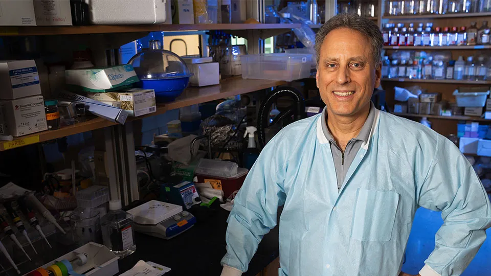
When Mark Prausnitz talks about his work as a professor, researcher, and entrepreneur, one theme comes through clearly: collaboration.
Prausnitz, a Regents’ Professor, Regents’ Entrepreneur, and J. Erskine Love Jr. Chair in the School of Chemical and Biomolecular Engineering, is this year’s recipient of the Class of 1934 Distinguished Professor Award.
“While I may be the focal point, it’s not a recognition of me as an individual. It’s a recognition of everything the team has done,” Prausnitz said. “I know how to do some things, but there are many things I don’t know how to do. That’s why working with others matters. You bring people together, fill in the gaps, and solve the whole problem.”
The “some things” Prausnitz knows how to do have led to revolutionary medical innovation over a 30-year career at Georgia Tech, where he has led transformative work in microneedle drug delivery, launching 10 companies in the process.
During that time, Prausnitz published hundreds of peer-reviewed papers, was granted dozens of patents, and advanced his work from early laboratory studies into more than 20 human clinical trials. His research has produced multiple FDA‑approved or clinically tested technologies.
Understanding Prausnitz’s success starts with his approach to engineering in practice. Science may begin with discovery, but engineering, as he describes it, focuses on taking something uncertain and making it work.
“One of the things that really distinguishes engineering from science is the work of problem-solving to reach an answer,” he said. “You start with something diffuse and figure out how to put all the pieces together. That to me is a hallmark of engineering.”
That way of thinking took shape early in his life.
News Contact
Julian Hills | Executive Communications Specialist
Institute Communications