Apr. 22, 2024

Effective July 1, Eric Vogel will become the executive director of the Institute for Matter and Systems (IMS), Georgia Tech’s newest Interdisciplinary Research Institute (IRI) that will launch on the same date.
As an evolution of the Institute for Materials (IMat) and the Institute for Electronics and Nanotechnology (IEN), IMS aims to enable convergent research at Georgia Tech related to the science, technology, and societal underpinnings of innovative materials and devices. Additionally, IMS seeks to integrate these innovations into systems that enhance human well-being and performance across information and communication, the built environment, and human-centric technologies that improve human health, wellness, and performance.
“Executive Vice President for Research Chaouki Abdallah and I are very excited about the launch of IMS, which positions Georgia Tech for integration of science and technology from atoms to devices, while explicitly drawing in researchers in the social sciences, design, business, and computing,” said Vice President of Interdisciplinary Research Julia Kubanek.
“IMS will ensure relevance across Georgia Tech through its newly configured Internal Advisor and Ambassador Board with representation across all six Colleges and GTRI,” she said. “Additional advisory committees representing IMS employees and facility users will ensure that we don’t sacrifice any of the research excellence for which IEN and IMat are known. With IMS I expect we will be even better positioned to tackle research problems that will have the greatest positive societal impact.”
Vogel will continue in his current position as the executive director of IMat until the launch of IMS. In addition to leading and growing IMat, Vogel is the Hightower Professor of Materials Science and Engineering at Georgia Tech’s School of Materials Science and Engineering, and he served as the IEN deputy director prior to leading IMat.
“It is an honor to be appointed executive director of the Institute for Matter and Systems, and I look forward to collaborating with the talented faculty and staff associated with it,” said Vogel. “This opportunity allows us to leverage the core competencies of IEN and IMat while extending our capabilities beyond nanotechnology and materials science. Together, we will be a hub for interdisciplinary research ranging from advanced materials to complex systems that solve global challenges.”
Georgia Tech’s IRIs facilitate collaboration between researchers and students from its six Colleges, the Georgia Tech Research Institute, national laboratories, and corporate entities to tackle critical topics of strategic significance for the Institute as well as for local, state, national, and international communities. IMS will also house and maintain the state-of-the-art Materials Characterization Facility and one of the largest academic cleanrooms in the nation, which offers a broad range of fabrication capabilities from basic discovery to prototype realization.
Before joining Georgia Tech in 2011, Vogel was an associate professor of materials science and engineering and electrical engineering at the University of Texas at Dallas. During this time, he also served as the associate director of the Texas Analog Center of Excellence and led UT Dallas’s involvement in the Southwest Academy for Nanoelectronics.
Prior to UT Dallas, he led the CMOS and Novel Devices Group and established the Nanofabrication Facility at the National Institute of Standards and Technology. Vogel holds a Ph.D. in electrical engineering from North Carolina State University and a B.S. in electrical engineering from the Pennsylvania State University. His research focuses on the development and fundamental understanding of electronic and nanomaterials and devices.
News Contact
Laurie Haigh
Research Communications
Apr. 16, 2024
More than 400 people participated in Energy Materials Day on March 27, as researchers and industry leaders came together to discuss and advance energy materials technologies such as solar energy, carbon-neutral fuels, and batteries.
Energy materials are the things — natural, manufactured, or both — that aid the use of energy. They also play a key role in developing cleaner, more efficient energy solutions.
Energy Materials Day was co-hosted by Georgia Tech’s Strategic Energy Institute (SEI), the Institute for Materials (IMat), and the Georgia Tech Advanced Battery Center. The event evolved out of last year’s Georgia Tech Battery Day.
“As an engine of innovation in science and technology, Georgia Tech has incredible opportunities and the responsibility to conduct research to benefit society,” said Chaouki Abdallah, executive vice president for Research at Georgia Tech. “We call this ‘research that matters.’”
Events like Energy Materials Day are part of an ongoing, long-range effort to position Georgia Tech, and Georgia, as a go-to location for modern energy companies. Tech was recently ranked by U.S. News & World Report as the top public university for energy research. Abdallah also outlined why Georgia Tech, with more than 1,000 researchers across campus working in the energy space, is a natural fit for events that foster collaboration between the public and private sectors.
“Right here, right now, we have the opportunity to harness our collective powers, our collective knowledge, our collective resources to become a global engine of innovation,” he said.
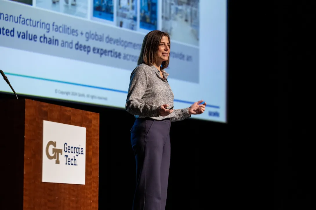
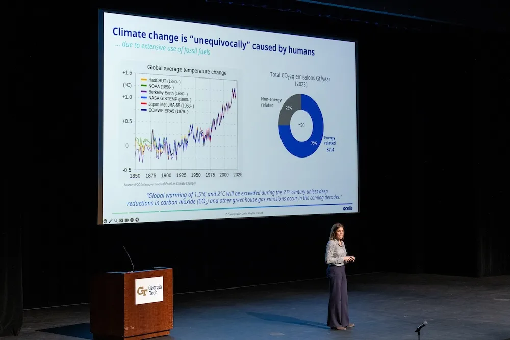
Plenary speaker Danielle Merfeld, global chief technology officer at QCells, highlighted opportunities for the current and future clean energy infrastructure in the United States.
"At the heart of our discussions today [are these questions]: What is new technology, and how do you make it ... and make it at scale, in an affordable, accessible, and reliable way?” she said.
"... [The] good news is this country has taken a very deliberate step toward creating the most robust industrial policy we've had in decades. ... This is driving opportunity and creating the foundation for manufacturing. So, [we can] use that industrial base of making and consuming power [and] decarbonize the electric grid by 2035...."
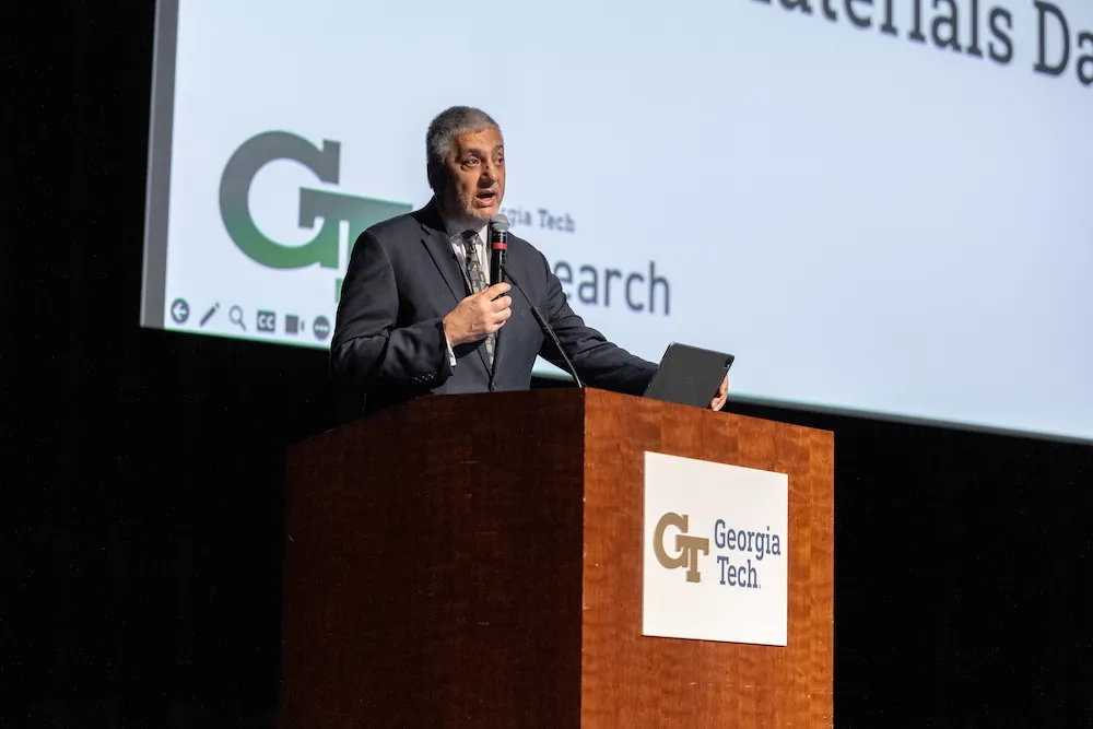
“Events like this are so important to forwarding progress in research and industry,” said Eric Vogel, IMat’s executive director. “It’s important to bring together professionals throughout the industry to keep these lines of communication open.”
The day was divided into three tracks: battery materials and technologies, photovoltaics and the grid, and materials for carbon-neutral fuel production. Attendees were encouraged to listen to talks from all three areas. Each track included academic speakers who shared their research and private-sector speakers who described how technological advancements are affecting the industry.
“With its rich history in energy research, Georgia Tech remains a leader in addressing global energy challenges,” said Tim Lieuwen, executive director of SEI. “The success of Energy Materials Day is encouraging, and I eagerly anticipate continuing these discussions in 2025.”
News Contact
Amelia Neumeister
Research Communications Program Manager
Mar. 21, 2024
Jud Ready, a principal research engineer at the Georgia Tech Research Institute (GTRI), has been selected to join the National Academy of Inventors’ (NAI) 2024 Class of Senior Members – a group of 124 academic inventors from NAI’s Member Institutions who have made significant contributions to innovation and technology.
Holding a dual appointment as Deputy Director of Innovation Initiatives for Georgia Tech’s Institute for Materials, one of Tech’s 10 Interdisciplinary Research Institutes (IRI) focused on advancing materials research and innovation, and with over two decades of experience as an adjunct professor in Tech’s School of Materials Science & Engineering, Ready has established himself as a leader in materials science and engineering.
Read the full story
News Contact
Michelle Gowdy
(Interim) Director of Communications, GTRi
Mar. 07, 2024

Matthew McDowell, Associate Professor in the George W. Woodruff School of Mechanical Engineering and the School of Materials Science and Engineering and initiative lead for energy storage at the Strategic Energy Institute
Matthew McDowell, Woodruff Faculty Fellow and associate professor in the George W. Woodruff School of Mechanical Engineering and the School of Materials Science and Engineering and initiative lead for energy storage at the Strategic Energy Institute, has received $1.3 million in funding through the Pioneering Railroad, Oceanic, and Plane Electrification with 1K energy storage systems (PROPEL-1K) program. Aimed at accelerating the electrification of the aviation, railroad, and maritime transportation sectors, PROPEL-1K is one of the latest ARPA-E grants with projects to develop energy storage systems that can achieve over 1,000 watt-hour per kilogram and 1,000 watt-hour per liter. These technologies will improve energy density fourfold over current technologies.
Inspired by fuel injectors in internal combustion engines and conventional flow batteries, McDowell’s project will advance an alkali hydroxide triple phase flow battery to enable reversible operation of ultrahigh-energy density battery chemistries. The project’s proposed design will increase energy density by leveraging innovative pumping and handling of molten alkali metal and hydroxide species to maximize the volume of reactants over inactive components.
McDowell will work with Asegun Henry, associate professor in the Department of Mechanical Engineering at the Massachusetts Institute of Technology (MIT). Prior to MIT, Henry was an assistant professor in the George W. Woodruff School of Mechanical Engineering at Georgia Tech.
Created in 2007, the Advanced Research Projects Agency-Energy (ARPA-E) in the Department of Energy advances high-potential, high-impact energy technologies. The agency focuses on transformational energy projects that can be meaningfully advanced with a small amount of funding over a defined period through a streamlined awards process that enables quick action and catalyzes cutting-edge areas of energy research.
News Contact
Priya Devarajan | SEI Communications Program Manager
Feb. 21, 2024

Energy is everywhere, affecting everything, all the time. And it can be manipulated and converted into the kind of energy that we depend on as a civilization. But transforming this ambient energy (the result of gyrating atoms and molecules) into something we can plug into and use when we need it requires specific materials.
These energy materials — some natural, some manufactured, some a combination — facilitate the conversion or transmission of energy. They also play an essential role in how we store energy, how we reduce power consumption, and how we develop cleaner, efficient energy solutions.
“Advanced materials and clean energy technologies are tightly connected, and at Georgia Tech we’ve been making major investments in people and facilities in batteries, solar energy, and hydrogen, for several decades,” said Tim Lieuwen, the David S. Lewis Jr. Chair and professor of aerospace engineering, and executive director of Georgia Tech’s Strategic Energy Institute (SEI).
That research synergy is the underpinning of Georgia Tech Energy Materials Day (March 27), a gathering of people from academia, government, and industry, co-hosted by SEI, the Institute for Materials (IMat), and the Georgia Tech Advanced Battery Center. This event aims to build on the momentum created by Georgia Tech Battery Day, held in March 2023, which drew more than 230 energy researchers and industry representatives.
“We thought it would be a good idea to expand on the Battery Day idea and showcase a wide range of research and expertise in other areas, such as solar energy and clean fuels, in addition to what we’re doing in batteries and energy storage,” said Matt McDowell, associate professor in the George W. Woodruff School of Mechanical Engineering and the School of Materials Science and Engineering (MSE), and co-director, with Gleb Yushin, of the Advanced Battery Center.
Energy Materials Day will bring together experts from academia, government, and industry to discuss and accelerate research in three key areas: battery materials and technologies, photovoltaics and the grid, and materials for carbon-neutral fuel production, “all of which are crucial for driving the clean energy transition,” noted Eric Vogel, executive director of IMat and the Hightower Professor of Materials Science and Engineering.
“Georgia Tech is leading the charge in research in these three areas,” he said. “And we’re excited to unite so many experts to spark the important discussions that will help us advance our nation’s path to net-zero emissions.”
Building an Energy Hub
Energy Materials Day is part of an ongoing, long-range effort to position Georgia Tech, and Georgia, as a go-to location for modern energy companies. So far, the message seems to be landing. Georgia has had more than $28 billion invested or announced in electric vehicle-related projects since 2020. And Georgia Tech was recently ranked by U.S. News & World Report as the top public university for energy research.
Georgia has become a major player in solar energy, also, with the announcement last year of a $2.5 billion plant being developed by Korean solar company Hanwha Qcells, taking advantage of President Biden’s climate policies. Qcells’ global chief technology officer, Danielle Merfeld, a member of SEI’s External Advisory Board, will be the keynote speaker for Energy Materials Day.
“Growing these industry relationships, building trust through collaborations with industry — these have been strong motivations in our efforts to create a hub here in Atlanta,” said Yushin, professor in MSE and co-founder of Sila Nanotechnologies, a battery materials startup valued at more than $3 billion.
McDowell and Yushin are leading the battery initiative for Energy Materials Day and they’ll be among 12 experts making presentations on battery materials and technologies, including six from Georgia Tech and four from industry. In addition to the formal sessions and presentations, there will also be an opportunity for networking.
“I think Georgia Tech has a responsibility to help grow a manufacturing ecosystem,” McDowell said. “We have the research and educational experience and expertise that companies need, and we’re working to coordinate our efforts with industry.”
Marta Hatzell, associate professor of mechanical engineering and chemical and biomolecular engineering, is leading the carbon-neutral fuel production portion of the event, while Juan-Pablo Correa-Baena, assistant professor in MSE, is leading the photovoltaics initiative.
They’ll be joined by a host of experts from Georgia Tech and institutes across the country, “some of the top thought leaders in their fields,” said Correa-Baena, whose lab has spent years optimizing a semiconductor material for solar energy conversion.
“Over the past decade, we have been working to achieve high efficiencies in solar panels based on a new, low-cost material called halide perovskites,” he said. His lab recently discovered how to prevent the chemical interactions that can degrade it. “It’s kind of a miracle material, and we want to increase its lifespan, make it more robust and commercially relevant.”
While Correa-Baena is working to revolutionize solar energy, Hatzell’s lab is designing materials to clean up the manufacturing of clean fuels.
“We’re interested in decarbonizing the industrial sector, through the production of carbon-neutral fuels,” said Hatzell, whose lab is designing new materials to make clean ammonia and hydrogen, both of which have the potential to play a major role in a carbon-free fuel system, without using fossil fuels as the feedstock. “We’re also working on a collaborative project focusing on assessing the economics of clean ammonia on a larger, global scale.”
The hope for Energy Materials Day is that other collaborations will be fostered as industry’s needs and the research enterprise collide in one place — Georgia Tech’s Exhibition Hall — over one day. The event is part of what Yushin called “the snowball effect.”
“You attract a new company to the region, and then another,” he said. “If we want to boost domestic production and supply chains, we must roll like a snowball gathering momentum. Education is a significant part of that effect. To build this new technology and new facilities for a new industry, you need trained, talented engineers. And we’ve got plenty of those. Georgia Tech can become the single point of contact, helping companies solve the technical challenges in a new age of clean energy.”
News Contact
Feb. 08, 2024
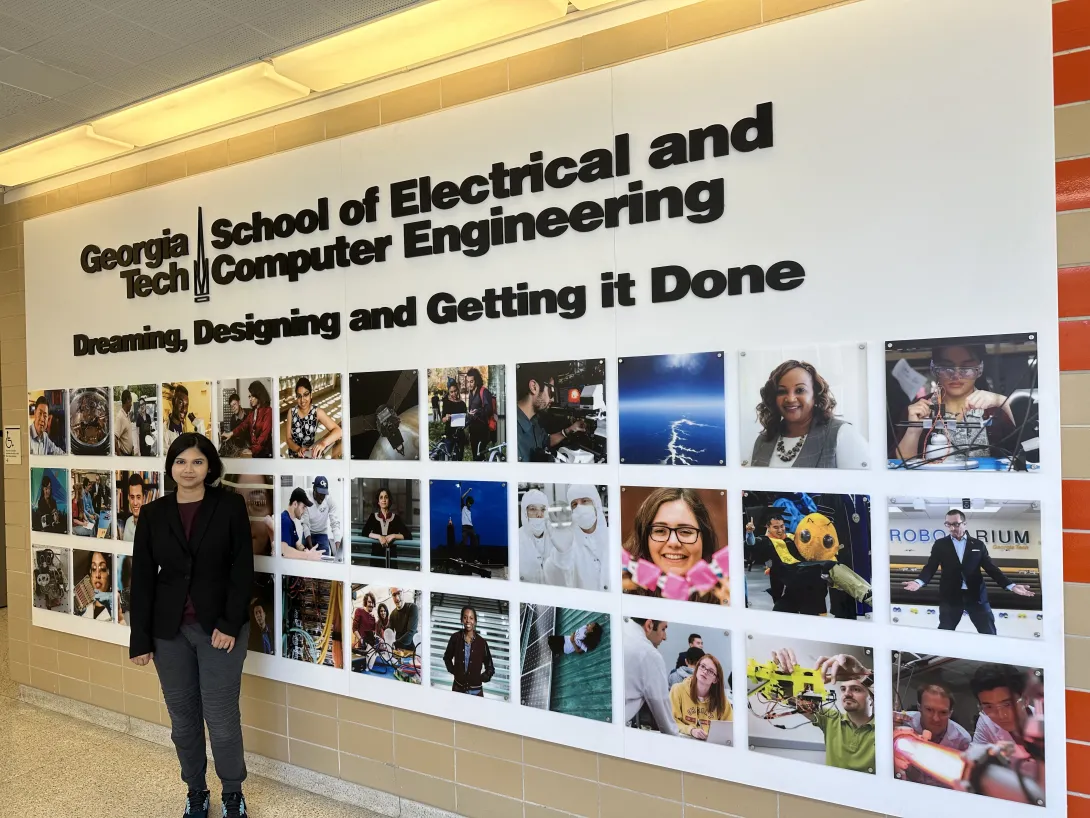
Georgia Institute of Technology School of Electrical and Computer Engineering Ph.D. candidate Fabia Farlin Athena received the prestigious Stanford Energy Postdoctoral Fellowship, becoming Georgia Tech’s first recipient of the distinction.
With climate change becoming one of the a defining issue of the 21st century, the transition to a low-carbon energy system will solve about three-fourths of the problem, according to the fellowship’s website. At the same time, the new energy system needs to be affordable, reliable, and available to the average person.
The three-year fellowship sponsored in Stanford’s Precourt Institute of Energy and Doerr School of Sustainability aims to identify, develop, and connect the next generation of energy leaders — from science and engineering to policy and economics — to translate theoretical climate change solutions into tangible realities.
At Stanford, Athena, who is advised by Eric M. Vogel in the School of Materials Science and Engineering, will work on emerging materials and devices for energy-efficient sustainable computing. She will be working with H.-S. Philip Wong, professor of electrical engineering, and Alberto Salleo, professor of materials science and engineering.
After being selected as a finalist, she presented her current Ph.D. research on adaptive oxide devices for energy-efficient computing, as well as her proposed research to the fellowship’s advisory board.
“It was an amazing experience to go through the selection process of writing the proposal and finally getting interviewed by the honorable advisory board,” Athena said. “It was humbling to get the opportunity to discuss my research with a person I have always looked up to in Professor Steven Chu, a Nobel Laureate in Physics and former U.S. Secretary of Energy!”
Athena is just one of 10 fellows selected globally this year. The fellowship provides her the opportunity to explore new and profound postdoctoral research that is distinct from her Ph.D. work.
“I am deeply grateful to my advisor Prof. Eric M. Vogel for his constant kind support throughout my Ph.D. and for believing in me,” Athena said. “He has been a pillar of constant support throughout my journey. I am also grateful to Prof. Samuel Graham for his kind constant support, including for this fellowship. I am thankful to my respected P.I.s at Stanford, Professor H.-S. Philip Wong, and Professor Alberto Salleo for their support of my proposal. I am also grateful to my respected mentors Prof. Suman Datta, Prof. William Alan Doolittle, Dr. Takashi Ando, and Dr. Vijay Narayanan for their kind support, advice, and opportunities. Finally, I would like to thank Georgia Tech ECE for providing the platform for learning, exploration, and collaboration.”
Before her time at Georgia Tech, Athena received her undergraduate degree in materials science and engineering from the Bangladesh University of Engineering and Technology. She then spent two semesters at Purdue University as a graduate researcher, where she collaborated with the Idaho National Lab on nuclear materials for next-generation energy.
Athena’s research has been recognized with the Georgia Tech ECE Ph.D. Fellowship, 2022 Cadence Diversity in Technology Scholarship, 2023 EECS Rising Stars, 2023 Colonel Oscar P. Cleaver Award for the most outstanding Ph.D. dissertation proposal in Georgia Tech ECE, 2023 MRS Graduate Student Award, and IBM Ph.D. Fellowship from 2022-2024.
News Contact
Zachary Winiecki
Jan. 26, 2024

Overhead view of the Re-Wind crew doing structural testing on a decommissioned wind turbine blade bridge on an industrial lot.
Pioneering a new recycling approach led to a big win for Re-Wind USA, a Georgia Tech research team led by Russell Gentry. The team has won the first phase of the Department of Energy's Wind Turbine Materials Recycling Prize, receiving $75,000 and an invitation to compete in the final phase.
"Our innovation for end-of-service wind turbine blades is both simple and elegant – at its core, our technology captures all the embodied energy in the composite materials in the blade," said Gentry, professor in the School of Architecture.
"The Re-Wind Network has pioneered structural recycling, the only of a number of competing technologies that upcycles the material of the blade and preserves the embodied energy from manufacturing," Gentry said.
"Little additional energy is used to remanufacture the blade and the life of the blade, typically 20 years, is extended at least 50 years. This is a win-win solution from an environmental and economic perspective."
Other methods for dealing with decommissioned wind blades involve mechanical grinding and landfilling of subsequent waste, an expensive and energy-intensive process, he said.
Team members include Gentry, Sakshi Kakkad, Cayleigh Nicholson, Mehmet Bermek, and Larry Bank, from the School of Architecture; Gabriel Ackall, Yulizza Henao, and Aeva Silverman, from the School of Civil and Environmental Engineering; and Eric Johansen, a business consultant from Fiberglass Trusses Inc.
The team is part of the Re-Wind Network, a multinational research and development network which develops large-scale infrastructure projects from decommissioned wind turbine blades.
Re-Wind's pedestrian bridges, known as BladeBridges, have already captured media attention. Two more BladeBridges are expected in Atlanta in 2024, Gentry said. Re-Wind has also developed, prototyped, and tested transmission poles made from blade segments. The team's other proposals include culverts, barriers, and floats.
News Contact
Ann Hoevel, Director of Communications, College of Design
Jan. 23, 2024
Valeria Tohver Milam leads the Macromolecular Materials at Biotic and Abiotic Interfaces research initiative for the Institute for Materials (IMat) and the Parker H. Petit Institute for Bioengineering and Biosciences at Georgia Tech. In this role, she is working to build an inclusive and active community across and beyond Georgia Tech to identify emerging research directions in macromolecular materials for biological and nonbiological applications. Milam is an associate professor in Materials Science and Engineering and a program faculty member of the Bioengineering graduate program at Georgia Tech.
In this brief Q&A, Milam discusses her research focus, how it relates to materials research, and the impact of this initiative.
What is your field of expertise and at what point in your life did you first become interested in this area?
My field of expertise lies in bio-inspired materials science and engineering. Natural macromolecular components of biological systems such as cell receptors or antibodies rely on recognition-based binding events to, for example, allow a cell to take up particular nutrients or to neutralize a specific pathogen threat. Inspired by nature’s capabilities, my group’s research strives to identify and study synthetic macromolecular materials with bio-inspired compositions and self-folded structures. I first became interested in using DNA for its recognition capabilities during my postdoc at the University of Pennsylvania. For the first several years as an assistant professor at Georgia Tech, my group used DNA duplexes as a temporary glue between particle surfaces. Our more recent efforts focus on finding oligonucleotides to function as ligands or capture agents for a specific biological or nonbiological target.
What questions or challenges sparked your current materials research?
Polymers or macromolecules hold a lot of promise as a class of materials for various applications. Synthetic macromolecules, however, pose a lot of synthesis and post-use challenges that can hinder the discovery and practical use of novel macromolecular chemistries. Natural polymers such as oligonucleotides and proteins, on the other hand, have their own elegant synthesis and degradation pathways. To promote discovery of novel macromolecular materials, my group uses nature’s reagents and building blocks to synthesize numerous artificial biopolymer candidates. Since we do not start with any sequence design rules, we rely on maximizing the composition diversity of these artificial biopolymers. We then test all candidates collectively to efficiently choose ones with the desired functionality.
Why is your initiative important to the development of Georgia Tech’s Materials research strategy?
One of the challenges to discovering macromolecular systems that are both novel and practical is the lack of design rules. For example, how does one choose the right number and composition of repeat units for a macromolecule that binds to a particular material surface or to a particular biological target. If you can take advantage of nature’s building blocks and enzymes, then you can explore a wide chemical combinatorial space without having to follow any prerequisite design rules. Better yet, you can then use your initial findings to come up with design rules to explore additional, possibly better macromolecular candidates. This approach to macromolecule discovery is inherently interdisciplinary since one must combine or adapt techniques and approaches developed by biologists, polymer scientists, and materials engineers. Thus, Georgia Tech is a great place to foster this interdisciplinary strategy to research.
What are the broader global and social benefits of the research you and your team conduct?
In addition to training members of our future workforce with interdisciplinary skill sets, we want to carve out a pathway to designing, synthesizing and using environmentally friendly, multiuse macromolecules with commercial promise.
What are your plans for engaging a wider GT faculty pool with IMat research?
Currently, we are primarily in the brainstorming stage. To this end, I am engaging with science and engineering faculty at GT as well as Emory. As cross-disciplinary ideas start to brew, we will work towards multi-PI funding opportunities that engage the broader GT faculty and community.
News Contact
Amelia Neumeister
Research Communications
Dec. 05, 2023

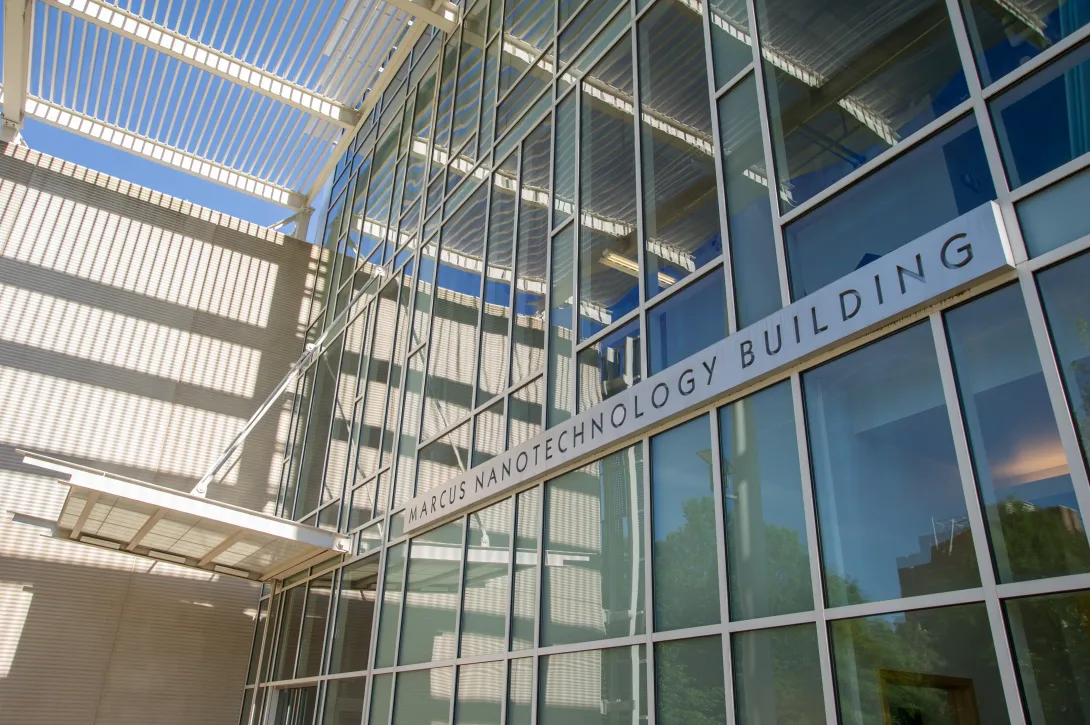
A new research center in the Institute for Electronics and Nanotechnology (IEN) will help bring together human-centered bioelectronics technology research to improve human healthcare and expand human-machine interface technologies.
The Wearable Intelligent Systems and Healthcare (WISH) Center will work to push innovation in wearable sensors and electronics technologies. Focus areas of the center will include electronics, artificial intelligence, biological science, material sciences, manufacturing, system design, and medical engineering.
“We are excited by the promise of bioelectronics improving human health and all the exciting science engineering that is required to make it a reality,” said Michael Filler, interim executive director of IEN.
WISH is directed by W. Hong Yeo, associate professor in Georgia Tech’s George W. Woodruff School of Mechanical Engineering and the Wallace H. Coulter Department of Biomedical Engineering at Georgia Tech and Emory, and Yuhang Hu, associate professor in the School of Chemical and Biomolecular Engineering at Georgia Tech.
“I founded WISH to bring together Georgia Tech’s expertise in various disciplines and to create opportunities for developing wearable bioelectronics and human-machine technologies leading to better lives and communities,” said Yeo.
Yeo’s research focuses on developing soft sensors, electronics and robotics for health monitoring and disease diagnosis at the intersection of human and machine interaction. Other researchers in the center represent disciplines from across Georgia Tech’s Colleges of Engineering, Computing, Sciences, Design, and Liberal Arts; Emory University; and Children’s Healthcare of Atlanta.
WISH will be one of IEN’s 10 strategic research centers, along with the 3D Systems Packaging Research Center, a graduated NSF Engineering Research Center focusing on advanced packaging using 2.5D and 3D heterogeneous integration technologies, and the Georgia Electronic Design Center, one of the world’s largest university-based semiconductor research centers. WISH is an evolution of the Center for Human-Centric Interfaces and Engineering, which received seed funding from IEN to focus on collaborative research for human-centered design, biofeedback control, and integrated nanosystems to advance human-machine interaction in the scope of healthcare.
IEN supports early-stage research in underfunded research areas that span all disciplines in science and engineering through its seed grant programs, which focus on research in biomedicine, electronics, optoelectronics and photonics, and energy applications.
News Contact
Amelia Neumeister, Research Communications
Nov. 17, 2023
The Institute for Electronics and Nanotechnology (IEN) and the Institute for Materials (IMat) have announced they will combine to form a new Interdisciplinary Research Institute (IRI) set to begin operations on July 1, 2024.
The new IRI, which has yet to be named, will explore the vast scientific, technological, societal, and economic impacts of innovative materials and devices, as well as foster their incorporation into systems that improve the human condition in areas such as information and communication technologies, the built environment, and human well-being and performance.
“The new IRI will not only combine the strengths of IEN and IMat, but will also allow us to further expand faculty representation from across the Institute,” said Julia Kubanek, vice president of Interdisciplinary Research at Georgia Tech. “As we look at the future of research in these areas, expanding inclusivity of researchers from the liberal arts, design, business, and basic sciences will allow us to better meet the education, workforce development, and innovation needs of Georgia, the U.S., and the world.”
The new IRI will strengthen Georgia Tech’s role in national focus areas such as the National Nanotechnology Initiative, the Materials Genome Initiative, and the CHIPS and Science Act, as well as identify and shape future priorities.
Core competencies of the new IRI will include:
- Fundamental science to comprehend and control matter from the nanoscale to the mesoscale.
- The synthesis, processing, and characterization of materials to achieve desired properties.
- The design and fabrication of novel devices and components with enhanced capabilities.
- The integration of materials, devices, and components into larger systems.
- Computing, modeling, simulation, and big data to advance progress at all length scales.
- Integration into all stages of research, from conceptualization to impact assessment, of economic, business, and social factors to ensure sustainable and equitable benefits.
“IEN and IMat have worked closely together for years, and there is overlap in the research areas we cover,” said Eric Vogel, IMat’s executive director. “This is an opportunity for us to build on IEN and IMat’s individual successes and our strong record of collaboration to create something even more exceptional.”
The new IRI will strengthen the state-of-the-art core cleanroom and characterization facilities, providing researchers with the tools and resources necessary for cutting-edge interdisciplinary research. These facilities will continue to serve both Georgia Tech and, through its leadership within the NSF National Nanotechnology Coordinated Infrastructure, the nation. Recognizing the importance of nurturing talent, it will champion education and outreach programs to inspire the next generation and equip the workforce with the skills necessary to collaborate and communicate across multiple disciplines.
“This is an exciting time to look to the future,” said Michael Filler, interim executive director of IEN. “We highly value the dedication and hard work of our staff and research faculty, who have been crucial to the success of IEN and IMat and will be the backbone of this new organization. We look forward to creating something exceptional in the coming months.”
News Contact
Laurie Haigh
laurie.haigh@research.gatech.edu