May. 02, 2024
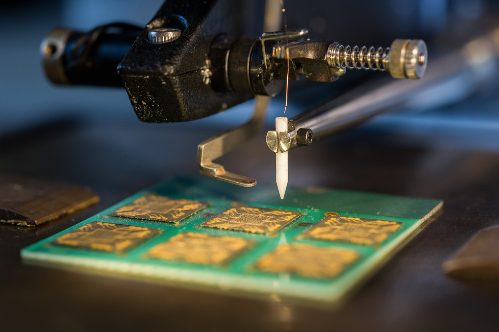
When Amy Bonecutter-Leonard was a second-semester undergraduate at the Georgia Institute of Technology, she applied for a work-study job in the cleanroom at the Microelectronics Research Center (MiRC). There, she learned process techniques for making the same type of electronic chips used in cellphones.
With this new knowledge, she could train and help other students with their research. At the time, Bonecutter-Leonard was a chemical engineering major with no plans to go into microelectronics. Working in the cleanroom changed that.
“I fell in love with microelectronics through exposure to the research and development work performed in the cleanroom,” she said.
What started as a student job led to her taking microelectronics classes — and eventually to a career in the field. “My work-study prepared me with hands-on technical skills I would have never learned from just being in a classroom,” she said. Now, Bonecutter-Leonard works as a microelectronics business chief engineer at defense contractor L3Harris Technologies.
Her story is one of many from the Institute for Electronics and Nanotechnology (IEN, the successor to MiRC), which has been training students from kindergarten to graduate school to be leaders in the microelectronics and nanotechnology space. The goal of IEN’s outreach is to make nanotechnology and microelectronics — such as computer chips and sensors — as accessible as any other science. Ultimately, these efforts will build up the U.S. workforce in the field, ensuring the country remains at the forefront of the technology that powers Americans’ everyday lives.
Building the Workforce
Bolstering the number of workers in the microelectronics industry is imperative to keep the U.S. globally competitive. Right now, 40% of the industry's labor force is older than 50, with practitioners aging out of their careers at a pace new talent cannot match. Additionally, heavy educational barriers to entry, including required degrees and specialized training, prevent more people from pursuing careers in the field. Without dedicated efforts, the entire sector — and the nation — will fall behind.
IEN is working to solve this pipeline problem.
“With the national semiconductor workforce aging, it is important now more than ever that we educate the next generation to move into these jobs,” said Michael Filler, IEN’s interim executive director. “IEN is proud to support the semiconductor industry by providing students with the interdisciplinary skills and hands-on technical training essential for success in this fast-paced, global field.”
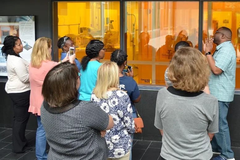
Georgia Tech is uniquely positioned to lead this charge with its 28,500 square feet of academic cleanroom space, the largest in the Southeast and among the largest in the U.S. From micro-electro-mechanical systems to electronics fabrication, workers have 100 bays in which to conduct leading-edge research. These cleanrooms are also key teaching and training facilities.
IEN invites anyone from around the world, whether affiliated with the Institute or not, to become a core user of the cleanroom facilities. The center also regularly hosts short courses for external partners — academic, industry, and government — in microfabrication and soft lithography for microfluidics. Over the past three years, more than 700 people went through new-user orientation, and 193 enrolled in the short courses.
Teaching the Next Generation
Making nanotechnology — of which microelectronics is an example — educationally accessible begins before college. Each semester, more than 800 K-12 students participate in IEN’s Introduction to Nanotechnology virtual lesson. Associate Director for Education and Outreach Mikkel Thomas begins his presentations by asking a simple question: What do you know about nanotechnology?
“About 99% of the time, they say that’s what makes Ironman’s suit work,” said Thomas. “That means they’ve learned the wrong lesson — that nanotechnology is a futuristic tech and that you have to be as smart as Tony Stark to work in the field.
“But most people interact with nanotechnology multiple times throughout their day, and they have no idea they're doing it.”
Thomas also emphasizes there is a career path for everyone, even if they don’t plan to get a traditional four-year degree. Part of IEN’s workforce development initiative is to build up the entire pipeline from industry and research lab technicians at the certificate level to postdoctoral researchers.
“It’s important for us to reach kids who don’t know what career options are available in nanotechnology,” Thomas said. “We want them to know that whatever they're interested in, there is a pathway for them.”
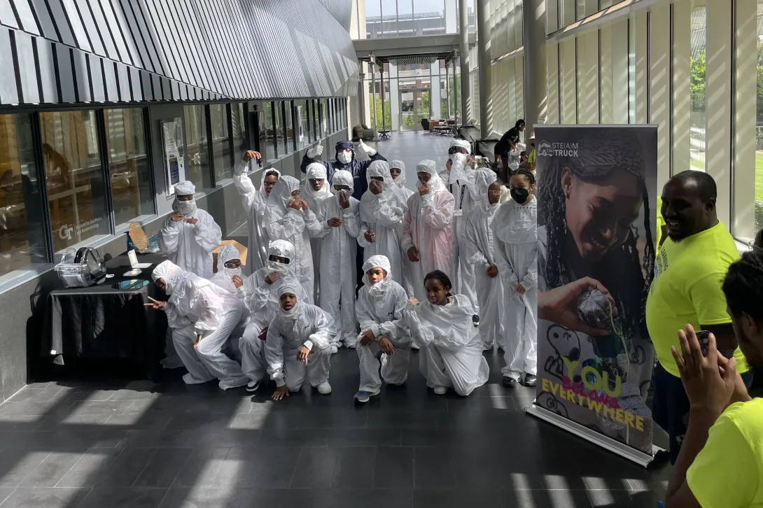
Sixth- through eighth-grade students sparked by this conversation can attend Chip Camp, a three-day STEM summer camp sponsored by Micron. They begin with a day at IEN to learn about thin films, magic sands, ferrofluids, and measuring their height in nanometers. The rest of the camp features hands-on visits to the Materials Characterization Facility (MCF) and the IEN cleanroom, where they can try on the white “bunny suits” technicians wear in the lab.
To further their reach, IEN’s workforce development team collaborates with teachers to bring nanotechnology into classrooms. During the summer, IEN offers the Research Experience for Teachers, a training program for public school and community college teachers to conduct nanotechnology research and learn how to incorporate it into their lessons. Middle school teachers have similar opportunities through the Nanoscience Summer Institute for Middle School Teachers.
Training the Workforce
When these students get to a university like Georgia Tech, IEN hires them for work-study jobs like the one Bonecutter-Leonard had. The hands-on cleanroom training is also vital to graduate students pursuing advanced degrees.
Katie Young earned her Ph.D. in materials science and engineering at Georgia Tech. Learning her way around the IEN cleanroom was essential for her graduate studies.
“My dissertation research involved synthesizing two-dimensional materials — only a single atom thick — for permeation barriers,” she explained. “I often used the cleanroom’s vacuum systems to synthesize and process 2D materials.” Now a research scientist at the Georgia Tech Research Institute, Young still works in the cleanroom on semiconductor device fabrication, building prototype quantum and biological sensors.
IEN opportunities are not limited to graduate research. Annually, about 150 Georgia Tech undergraduate students take microelectronics packaging and devices classes, with labs taught by IEN staff in the teaching cleanroom. These courses include Integrated Circuit Fabrication (ECE 4452), in which students learn to fabricate circuit elements, and the Science and Engineering of Microelectronic Fabrication (ChBE 4050/6050, open to graduate students as well), for students interested in semiconductor materials and fabrication.
Students don’t need to enroll at Georgia Tech to benefit from training, courses, and other opportunities. IEN’s internship program provides technical college students with training to become microelectronics technicians, either through work in the Biocleanroom or in the MCF.
Empowering Future Innovators
IEN also participates in the National Science Foundation Research Experiences for Undergraduates (REU), which provides opportunities for students from underrepresented groups or who attend schools without similar facilities. While enrolled at another university, John Mark Page was introduced to Georgia Tech’s cleanroom through an REU.
“That was my first exposure to any facility of this kind, and it felt like I was looking at the future. Being in a facility that can fabricate devices at or near the atomic level — it was hard to fathom,” Page said. “I had never thought that participating in microelectronics and nanotechnology as a student, especially as an undergraduate, was something I could do.”
As a result of his REU, Page transferred to Georgia Tech — he will graduate this summer with a bachelor’s degree in electrical engineering. He also completed a second REU at the University of North Carolina at Chapel Hill, worked as a student assistant in the IEN cleanroom, and participated in a Vertically Integrated Project (VIP), Chip Scale Power and Energy.
“I was interested in the VIP because it allowed me to spend more time in the cleanroom, familiarizing myself with semiconductor fabrication methods and training on new fabrication equipment,” Page explained. His experiences inspired him to consider a future career in the semiconductor industry.
“It wasn’t only the 10-week experience of the REU that made a lasting impact on me,” he said. “It was also the relationships formed with the people of IEN. The staff there are exceptional representatives of Georgia Tech, and they make IEN a tremendous asset to the future of microelectronics and nanotechnology in the U.S.”
Biya Haile, an ECE Ph.D. student, had a similarly meaningful REU experience. Haile, whose research focuses on creating micro-electro-mechanical systems-based sensors (MEMS), described the REU as “immersive.”
“The REU project enabled me to study chemical micro-sensor technologies, as well as state-of-the-art additive nano-manufacturing techniques, which has contributed to my research,” he said. “I feel lucky that my academic journey has entailed developing new technologies that use nanoscience to solve big problems.”
While Haile is currently focused more on designing and testing rapid processes for fabricating MEMS-based devices, he still occasionally works in the cleanroom on fabrication. He plans to go into the microelectronics industry after graduating.
The Path Ahead
All of IEN’s training and educational offerings align with IEN’s mission to bolster and diversify the microelectronics workforce, according to George White, senior director of strategic partnerships for the Georgia Tech research enterprise. “IEN has been at the forefront of the CHIPS infrastructure buildout, particularly in the area of education and workforce development,” he noted.
IEN’s efforts impact not just Atlanta but the entire country. Georgia Tech’s leadership in microelectronics research trains the innovators and practitioners of the future everywhere and ensures that America stays at the forefront of leading-edge technology. As demand increases for microelectronics, IEN is moving to meet it.
Effective July 1, 2024, the Institute for Electronics and Nanotechnology and the Institute for Materials will evolve into the Institute for Matter and Systems (IMS). This strategic union aims to foster convergent research at Georgia Tech, focusing on the science, technology, and societal underpinnings of cutting-edge materials and devices. Eric Vogel will be the director of IMS, and Michael Filler will be the deputy director.
